Quantcast
Channel: ElgensRepairs
Viewing all 33 articles
Browse latest View live

Namco/Bally Midway Galaga Repair Log

$
0
0
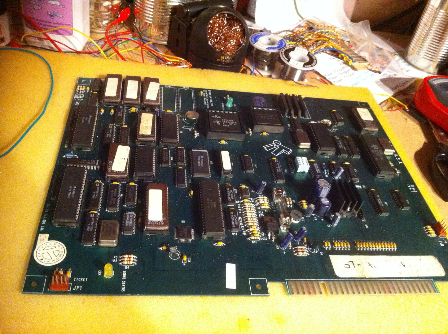
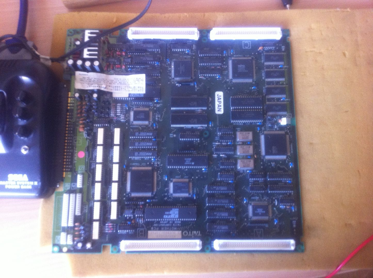
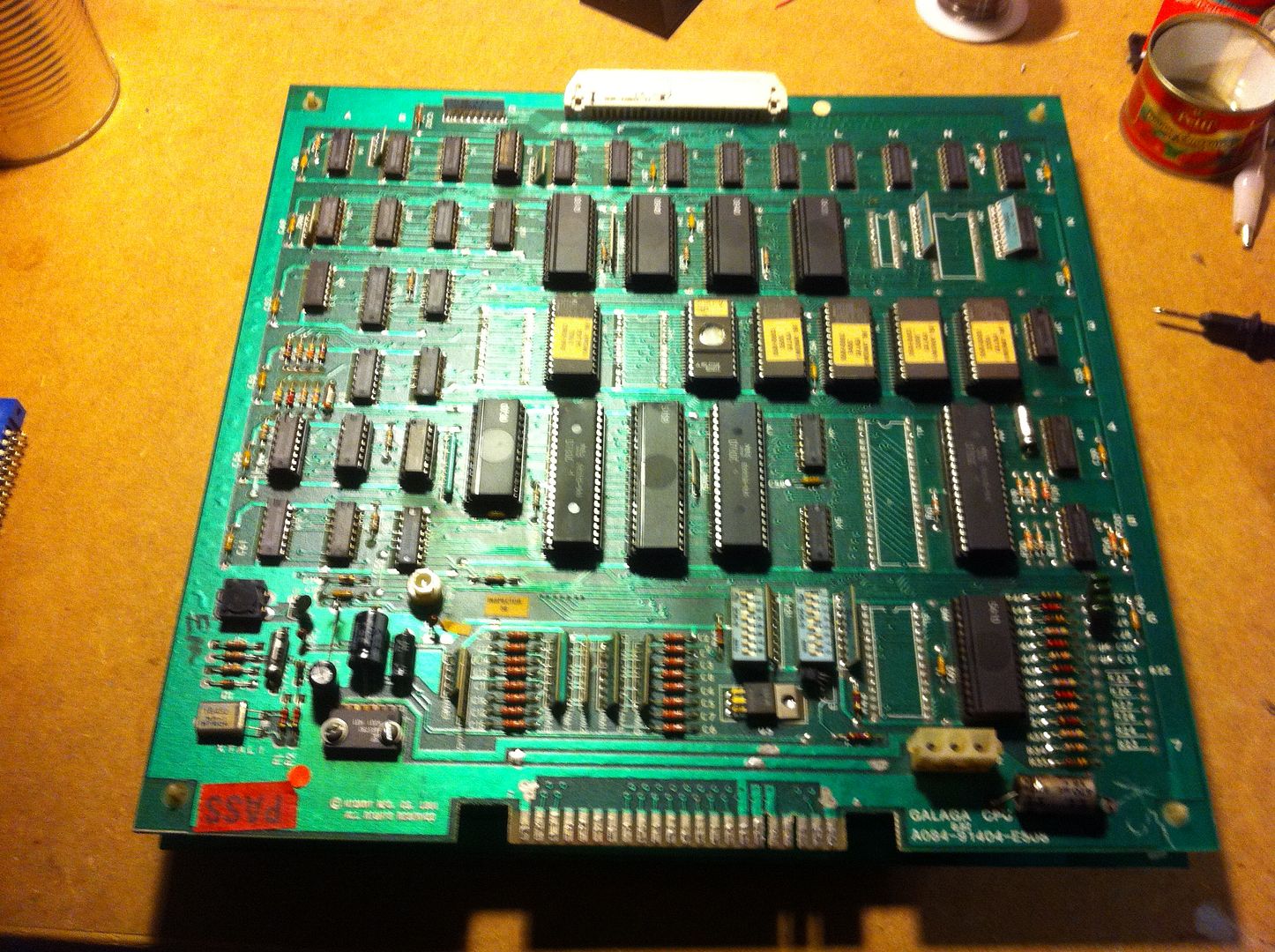
My dear friend (and also active user on many UK and Danish forums) Muerto asked me to have a look at his original Namco/Bally Midway Galaga. When he bought it years ago, he tested it and found that some of the sprites were displayed twice on screen. So it was put on a shelf and have been sitting there just waiting for someone to have a go at trying to repair it. When it arrived on my bench, it looked like this


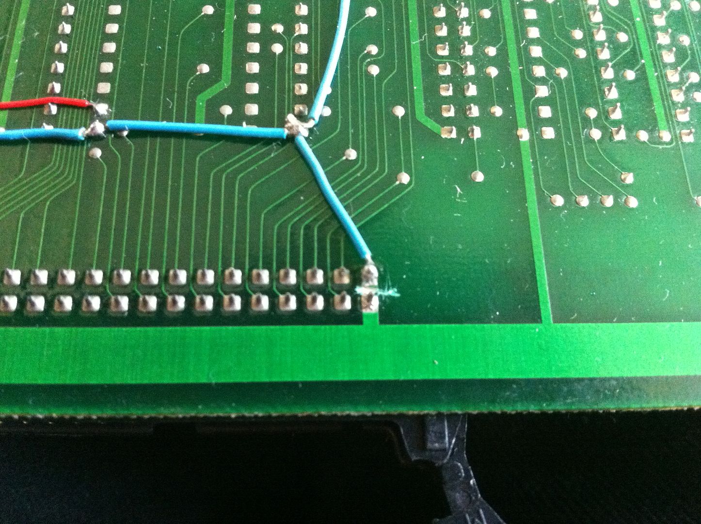
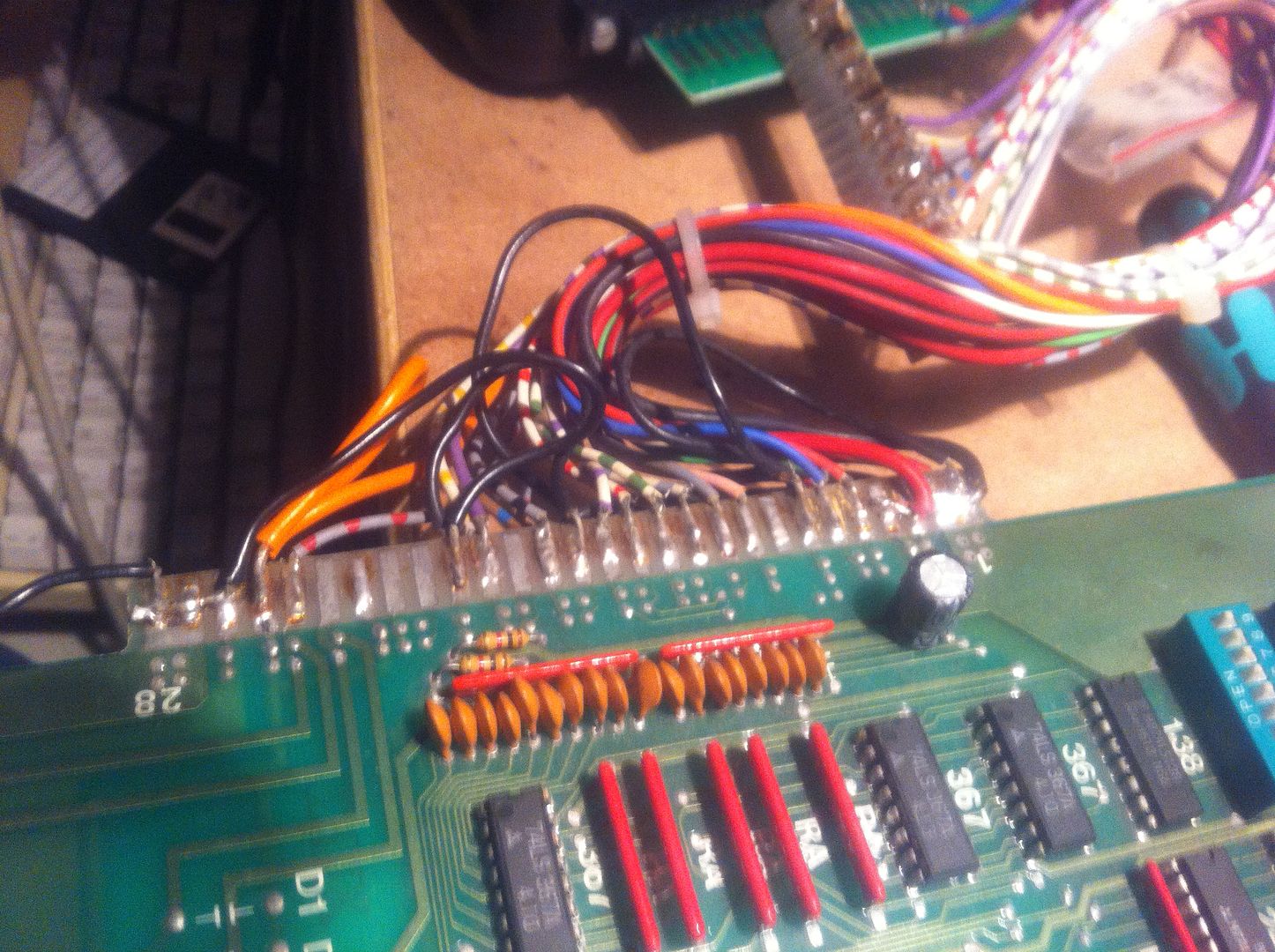
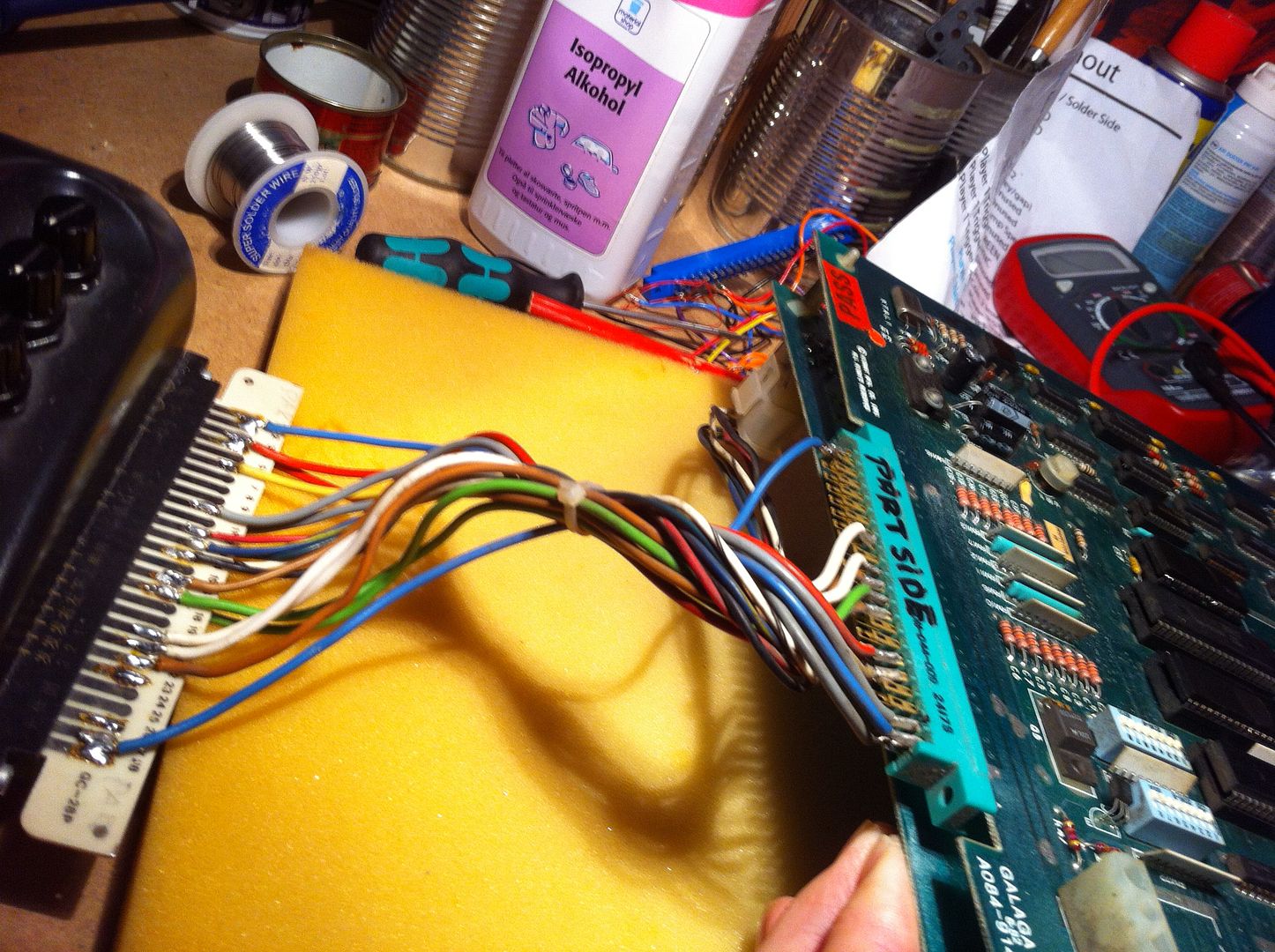
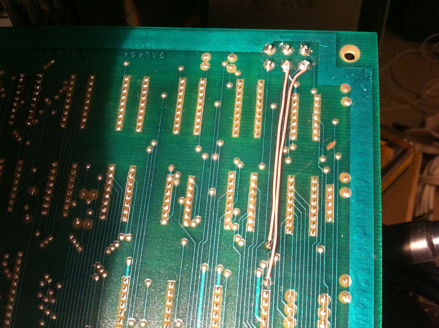
The board doesn't have video connections at the edge connector; they must be drawn from a molex on the video board


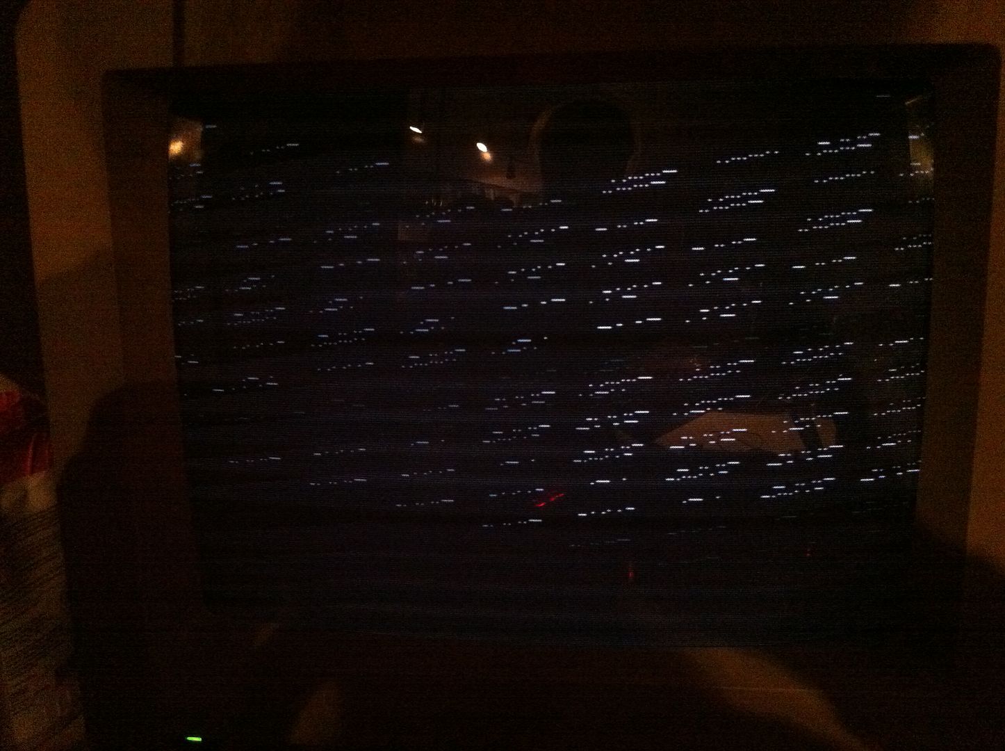
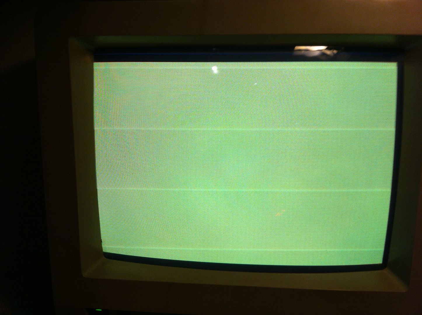
I didn't have a plug to fit this molex, so I cheated a bit, and soldered 4 wires (R, G, B, and sync) directly onto the solderside of the board along with the other wires from the edge connector. I fired it up, and got this


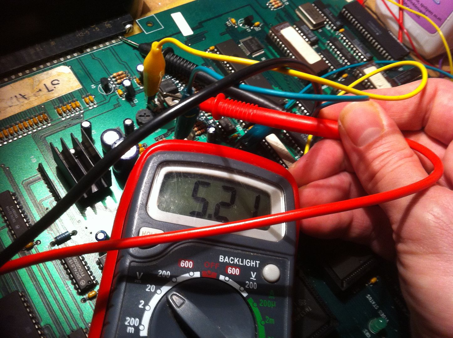
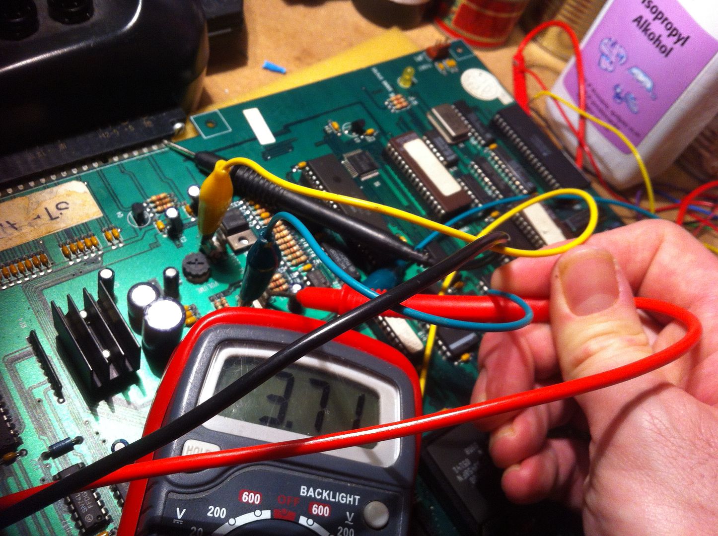
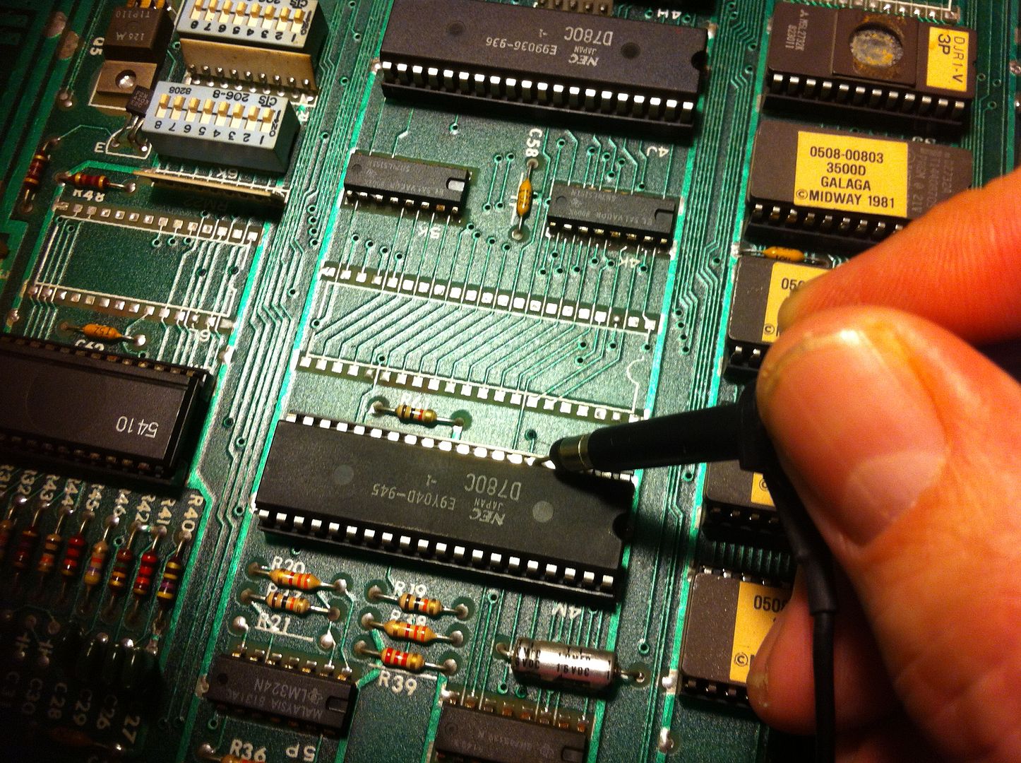
A solid yellow-ish screen and no sound at all };-( So I started examining the main CPU (this board has 3 x Z80 CPUs) for CLOCK signal


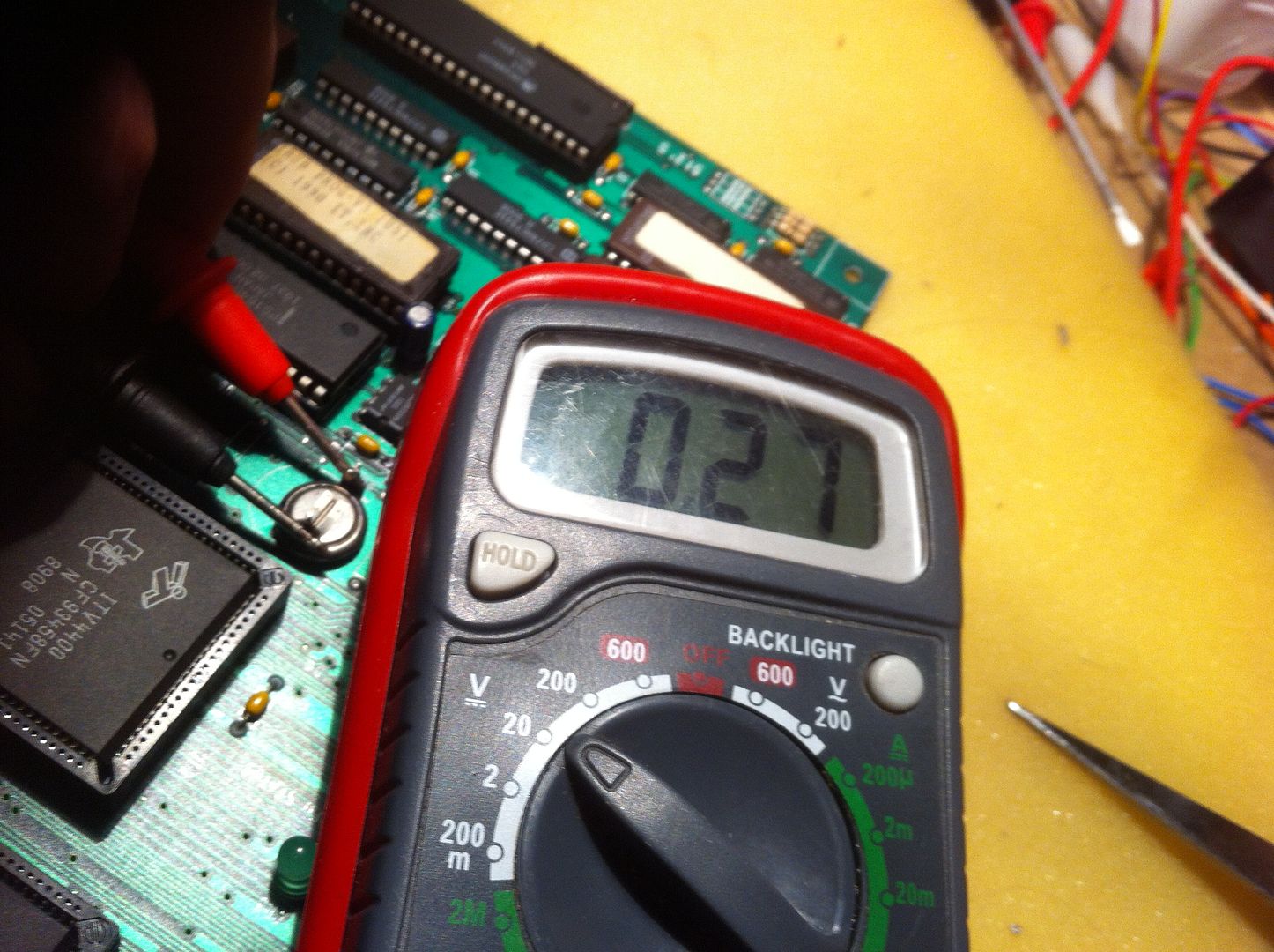
Hmmm, looks nice and healthy. Next up was the RESET signal


The signal jumped low about 2 or 3 times a second... the watch dog was barking ever so loudly! At this point, it's always good to check the ROMs, so you can rule out any software error from the equation; So be it!


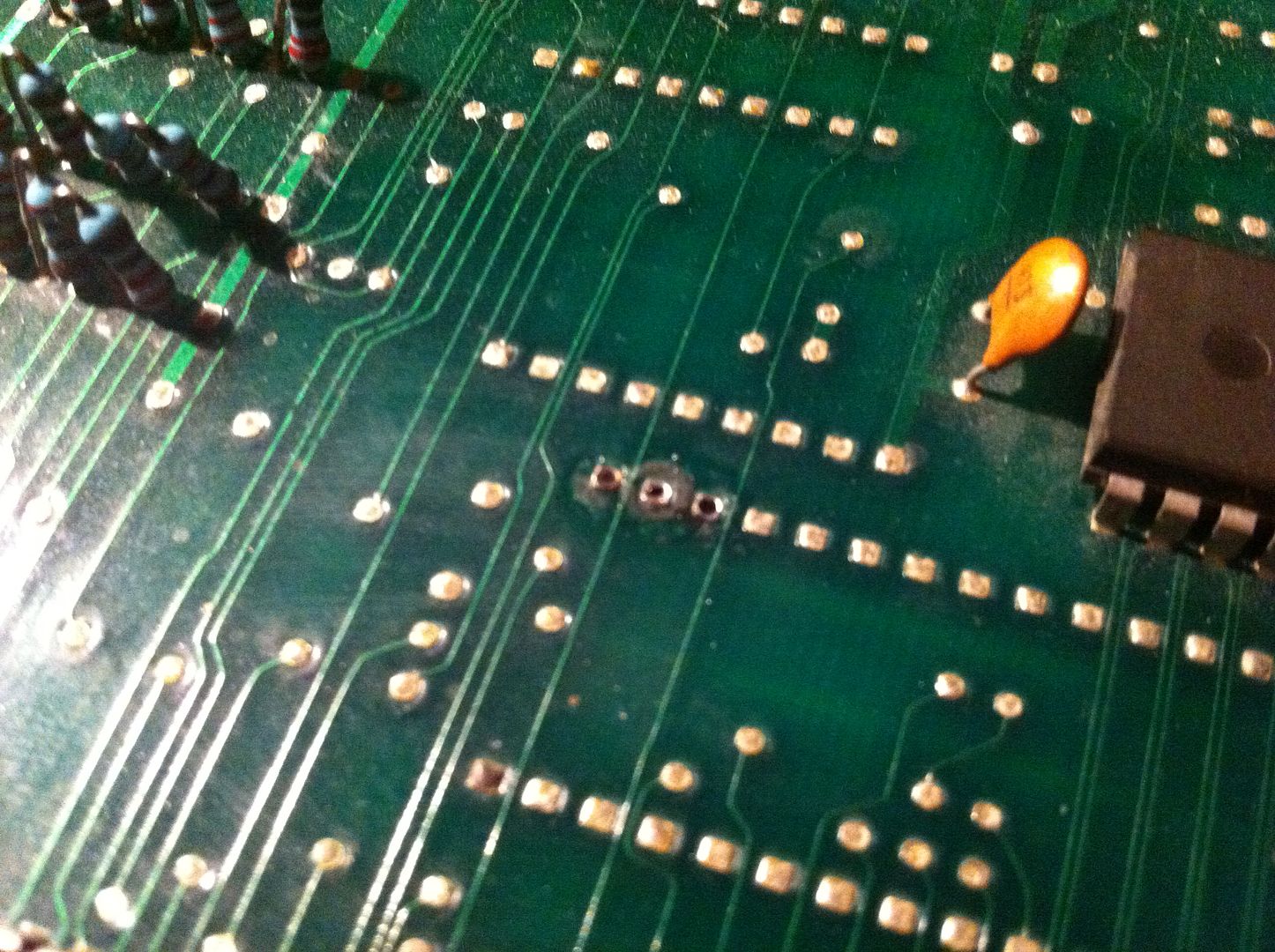
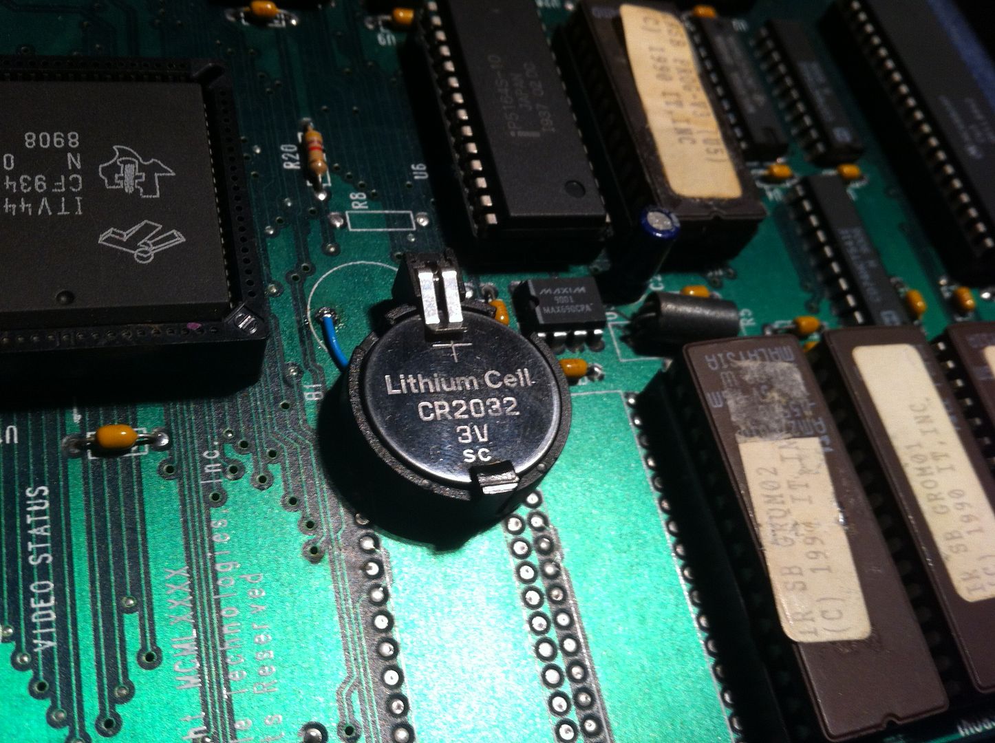
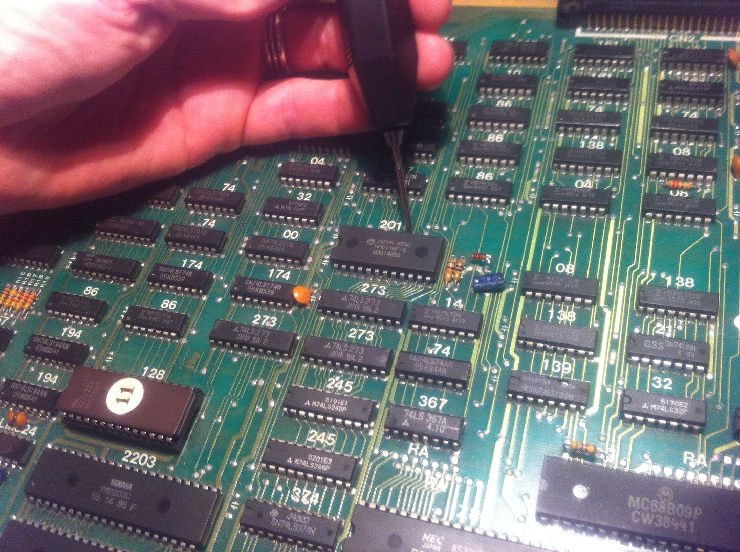
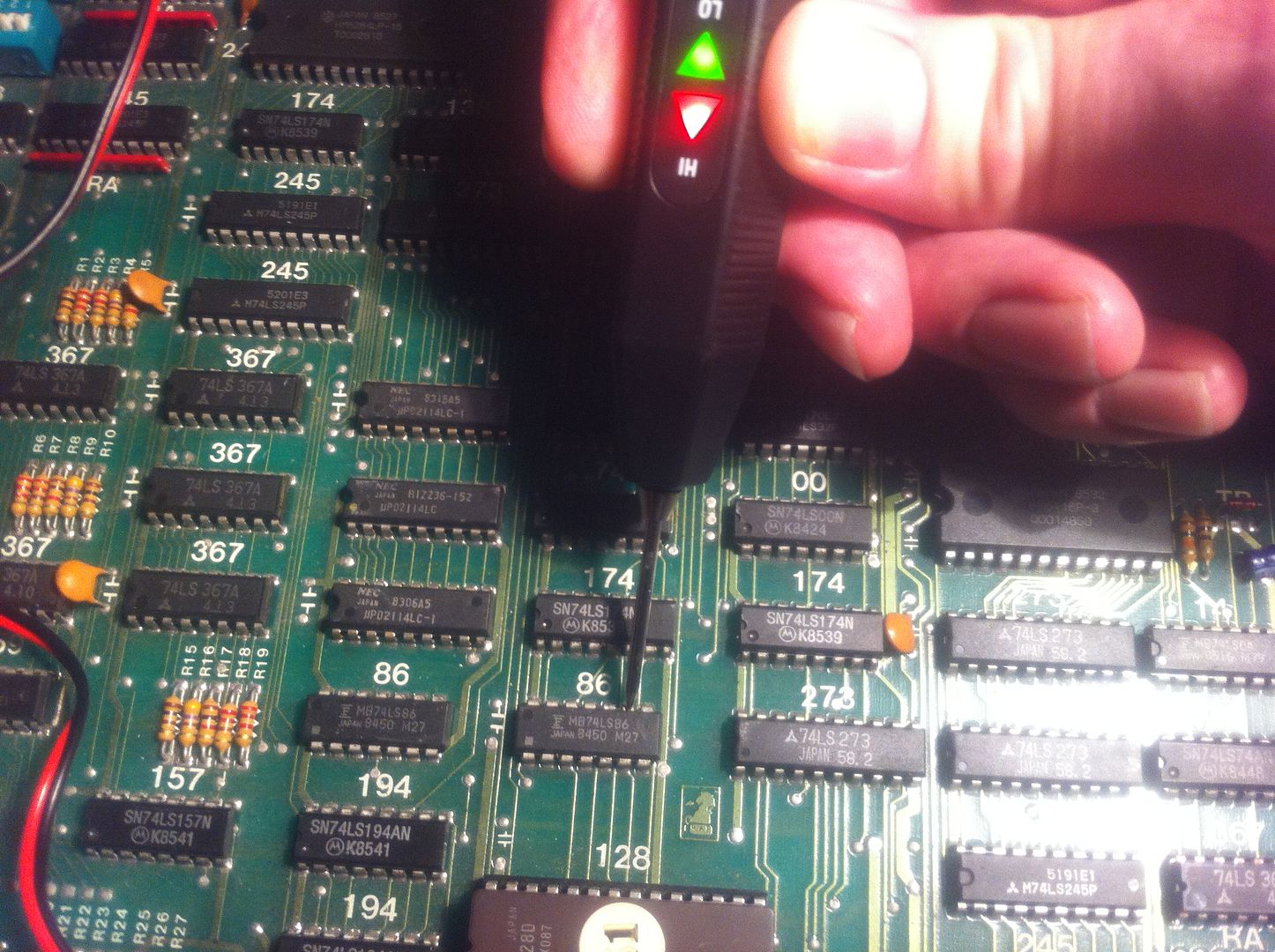
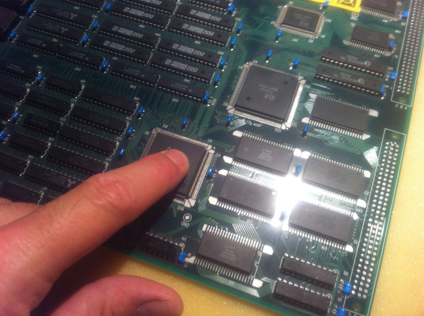
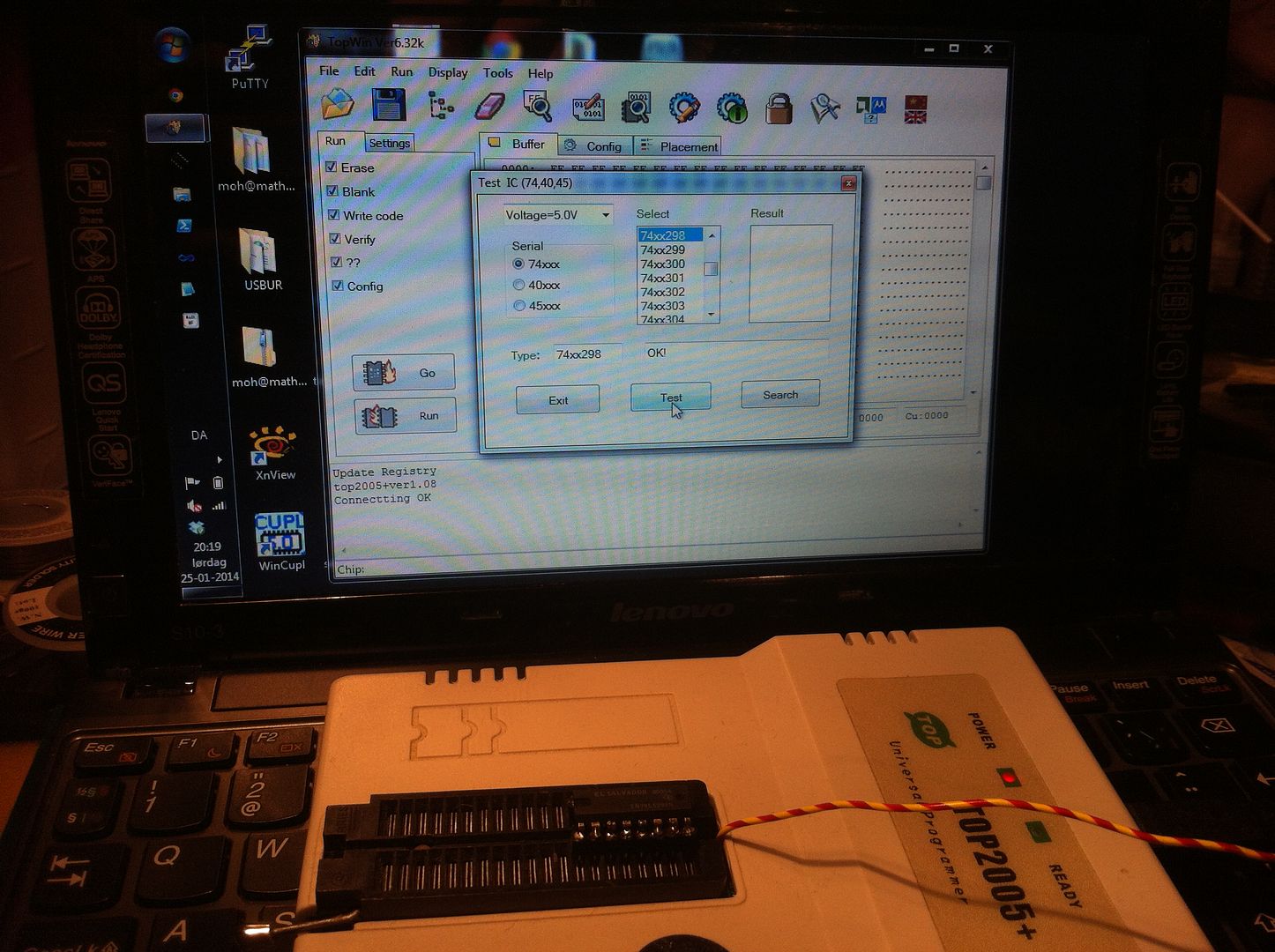
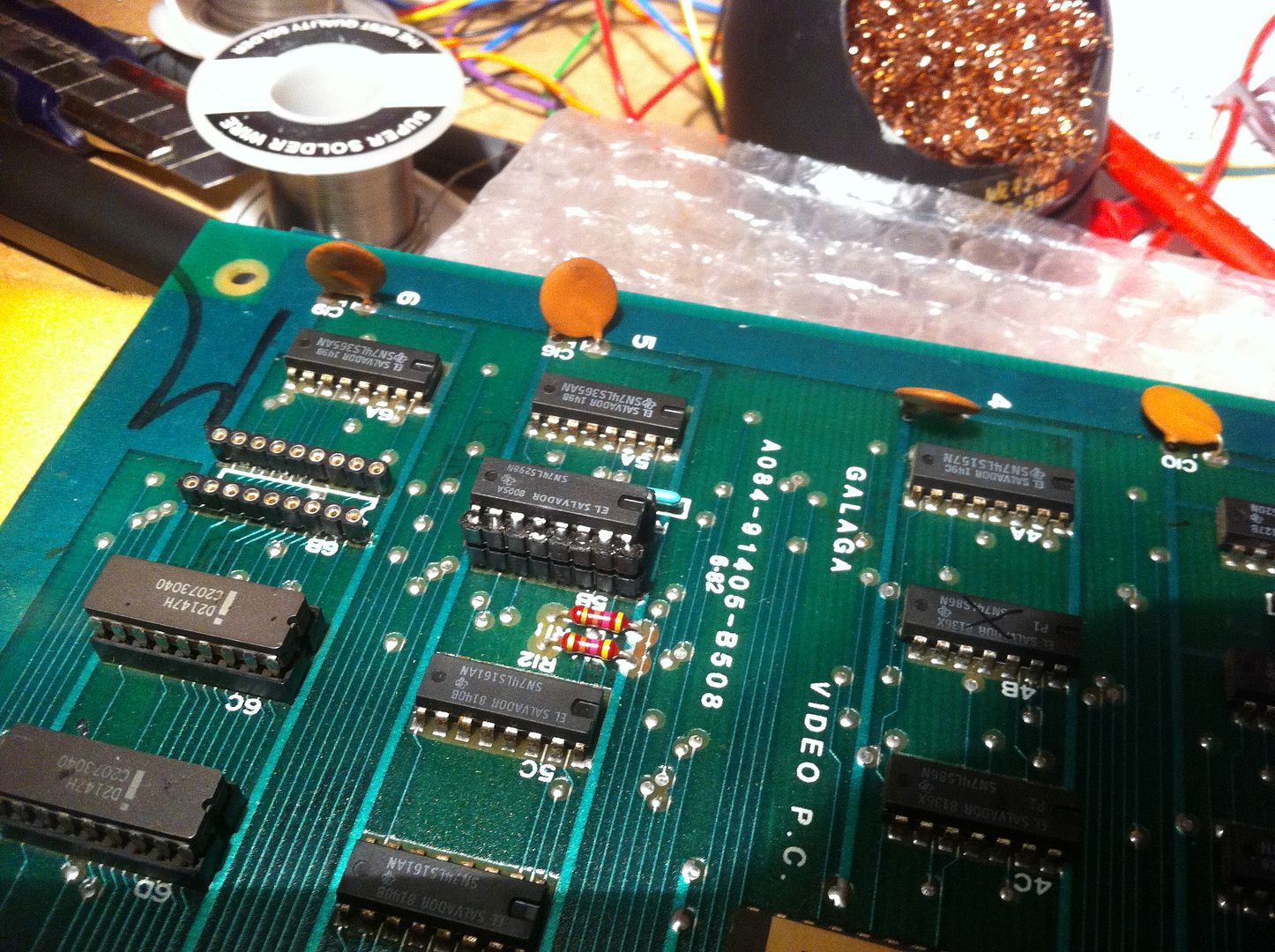
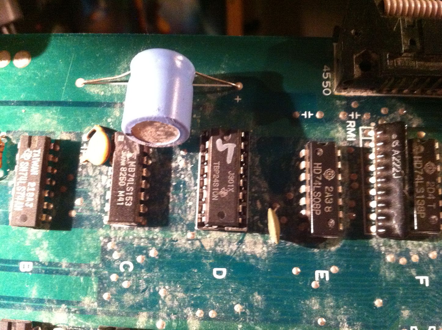
They all seemed to be in good shape and verified nicely against MAME. It was then I started to have a closer look at the custom ICs on this board


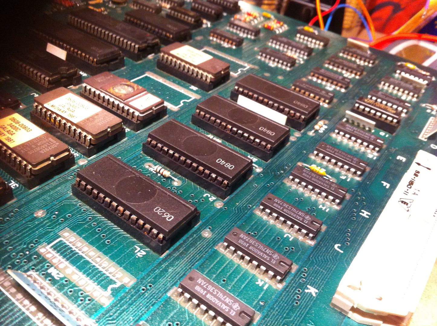
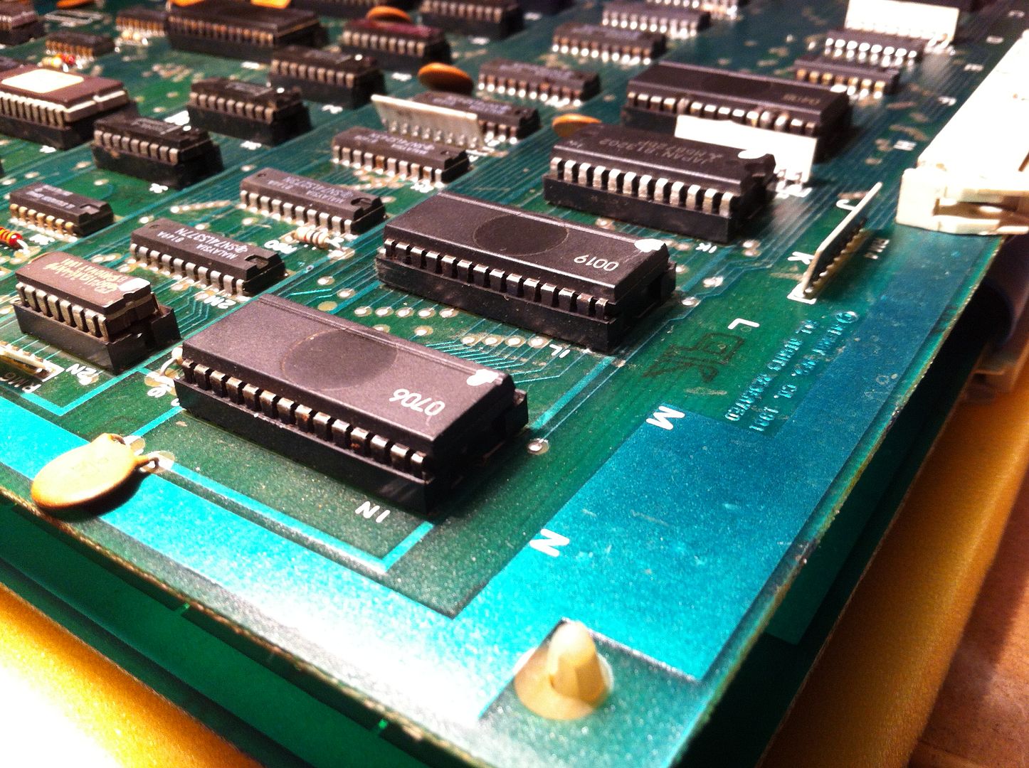
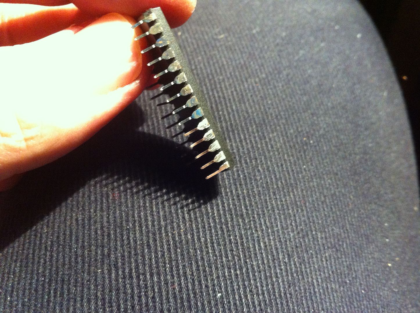
All of them, with no exception, had extremely corroded pins! And when trying to gently free the poor customs from their sockets (with my trusty flathead screwdriver), some of them lost a pin or two due to the extensive amount of corrosion


(the last two photos above are taken AFTER I've cleaned the ICs from the corrosion)
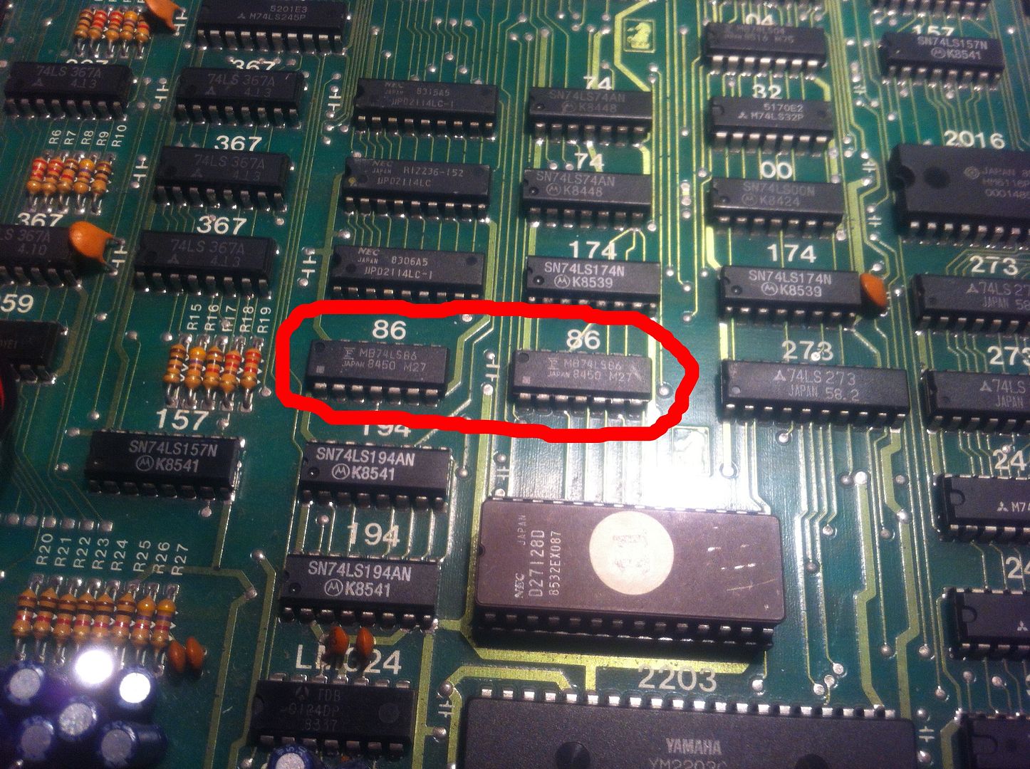
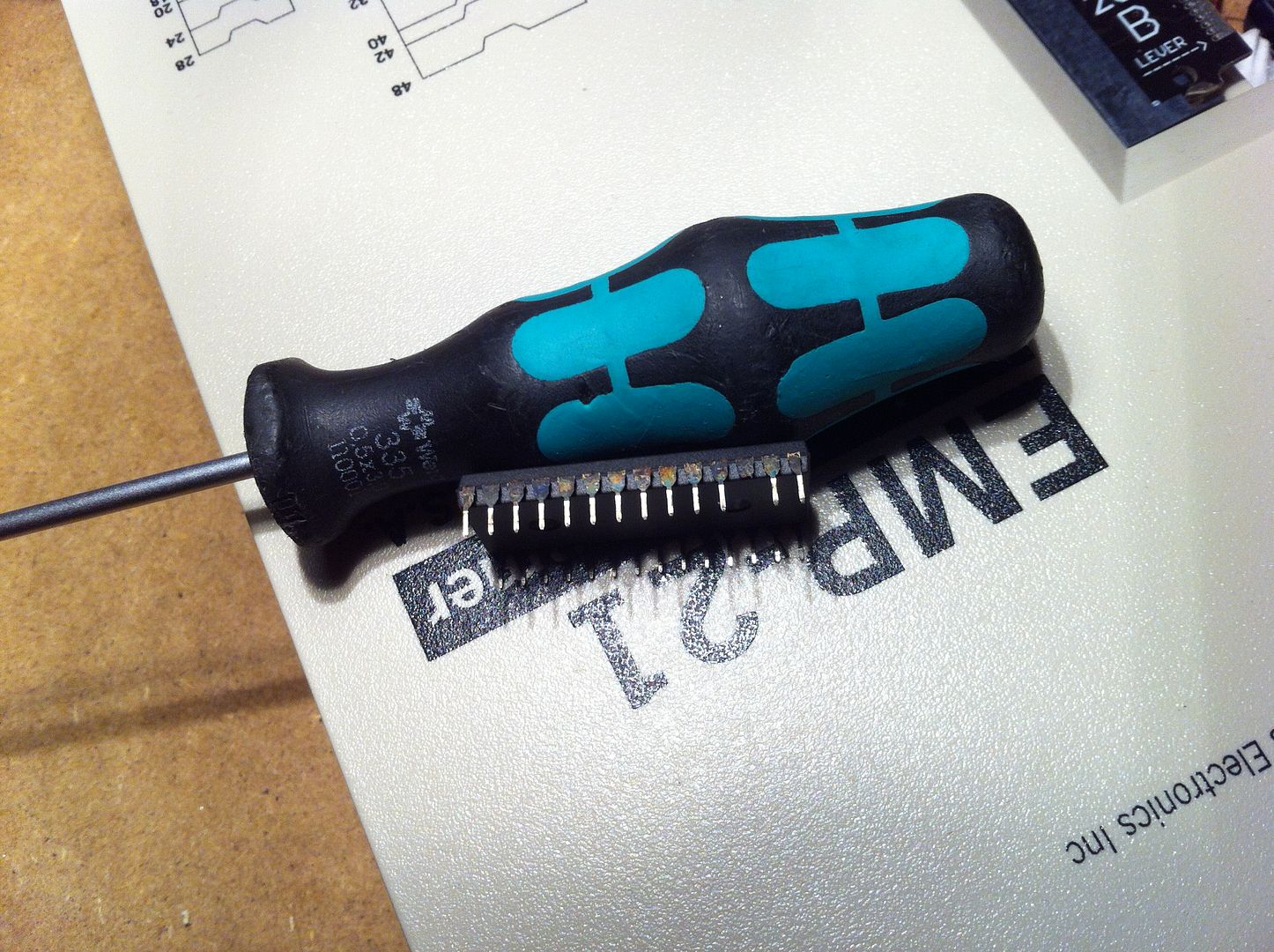
The first two ICs, I cleaned as I usually do by scraping the corrosion off using a Stanley knife. Next I patched new pins (taken from scrapped ICs) on where they had broken off and then gave all the pins a thin layer of solder.


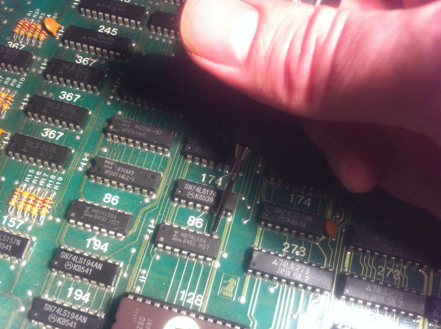
Ready to be plugged into the socket again! };-P Now the Stanley knife-method works well, but for 10+ ICs it becomes quite cumbersome. So after the two first customs it suddenly struck me! I remembered, that my lovely Dremel (How can any man live without one? Still think that every boy should be given one at birth: Congrats Daddy, it's a healthy boy, and here's his Dremel; please keep it safe until he's old enough to use it!) actually come with a steel brush, that I didn't have had the opportunity to use yet. So fitted the brush and tried carefully and at the slowest possible speed


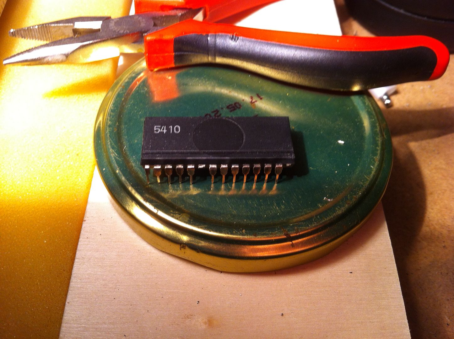
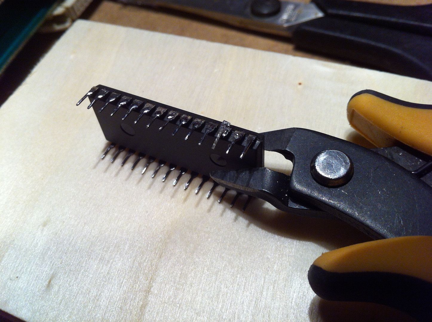
The result was simply fan-frakking-tastic! };-P


And each pin only took about 2-3 seconds to clean! };-O So I spend an evening cleaning ICs and patching up broken pins on the main board. With one of the ICs a broken piece of pin actually got jammed in the socket


So I had to desolder the socket


and fit a new one


When I was finished with cleaning ICs on the main board, I decided to try and hook it up in the test rig again. However, in the meantime I had gotten hold of a cheap original defective Namco/Bally Midway Pac-Land with an adaptor for some obscure standard that I haven't seen before


(properly some Belgian standard, as the seller (eBay) was from Belgium).
Now Pac-Land and Galaga uses the same pinout, and in particular the same molex for video, so I desoldered the obscure finger board, and fitted a JAMMA one.


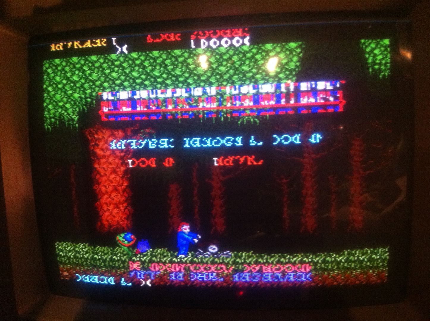
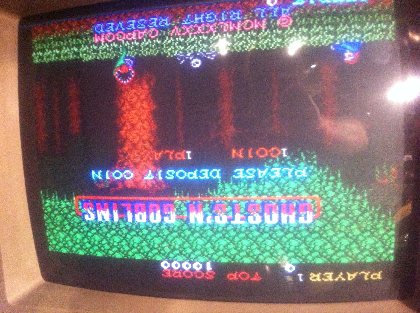
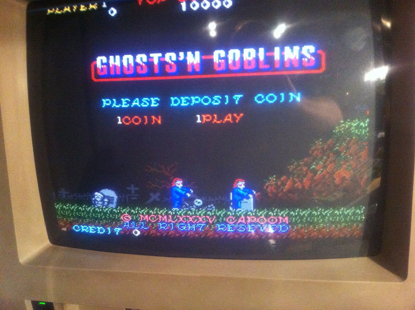
And when I flipped the switch, there was movement on the screen... the board self test. And after the test completed, the attract mode started playing with sound and all


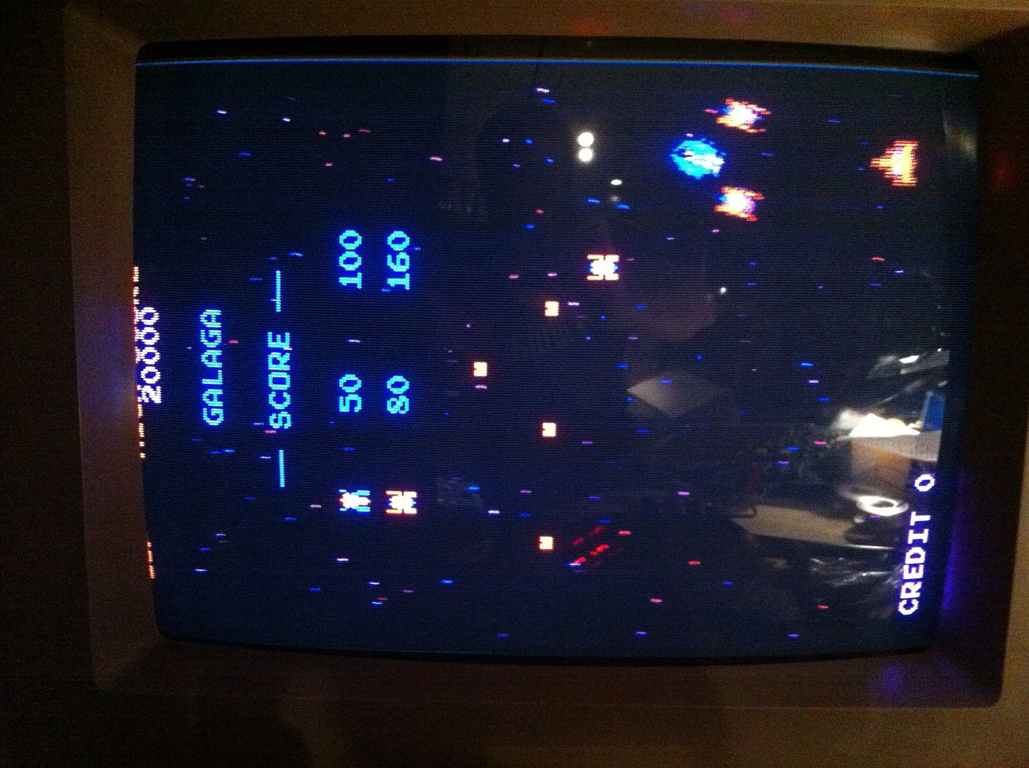
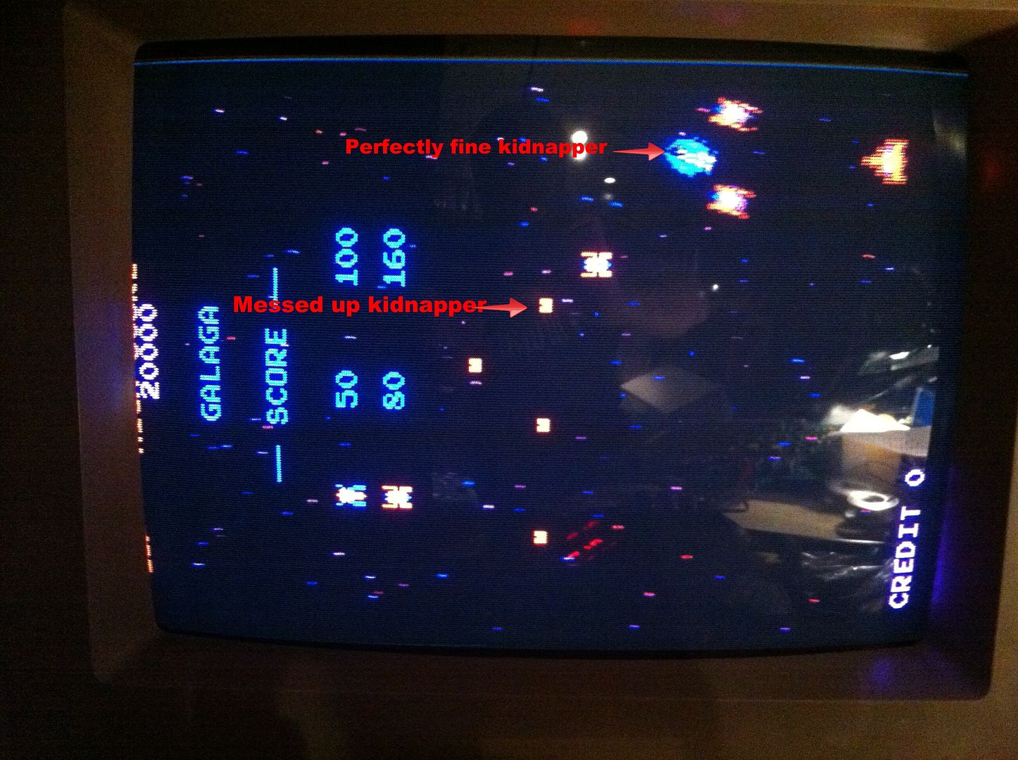
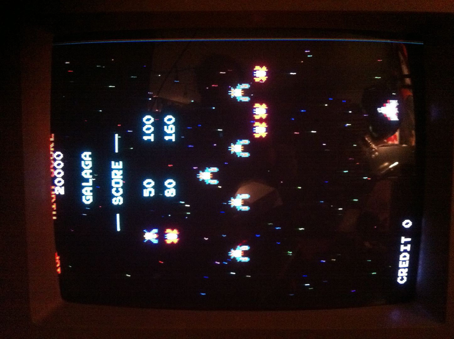
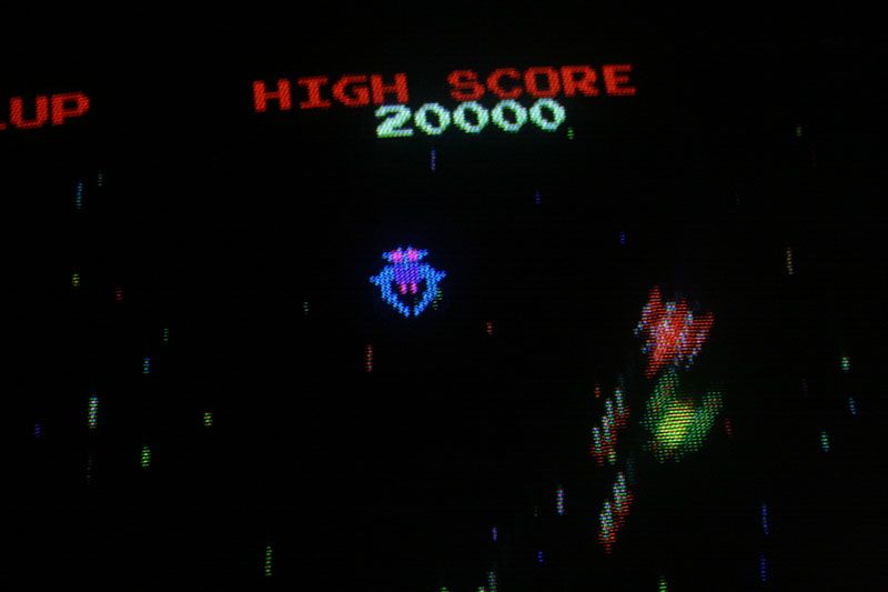
Now this was progress for sure! However, the screen was kind of purple-ish (doesn't show that well on the photos because of the quality of my iPhone camera and the quality of me as a photographer) and the "kidnappers" (the ones the can capture your fighter) only showed up as square red dots when hovering on the top of the screen. But when they did a dive, they looked perfectly fine.


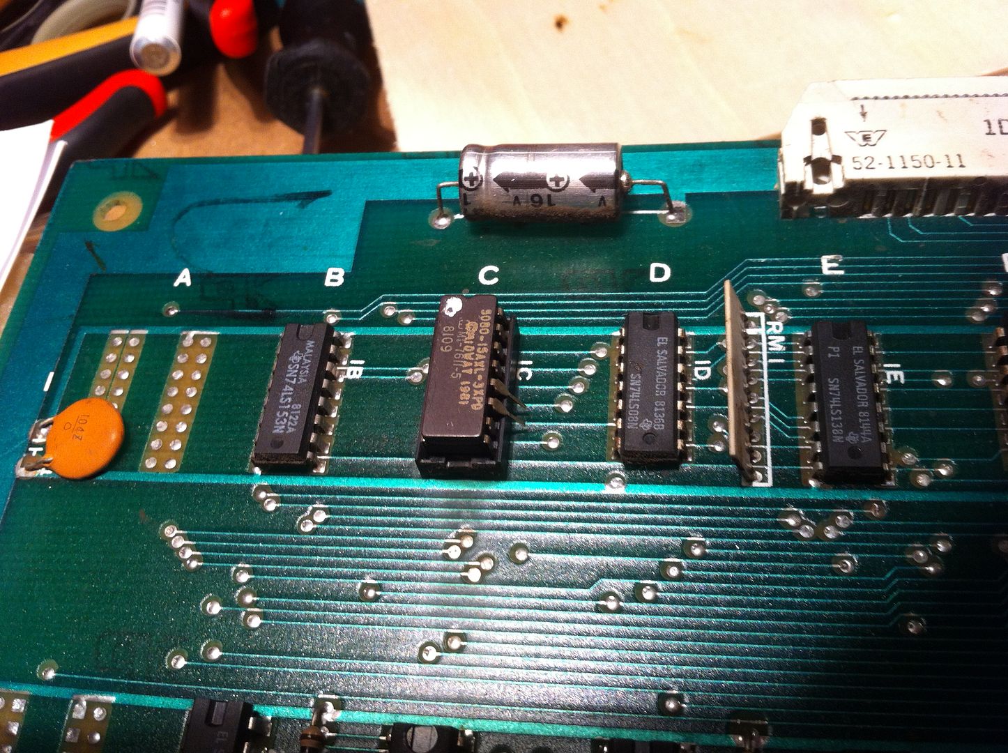
With all the customs on the video board was also corroded, I still hoped that a clean-up there might fix the problems. So yet again I spend an whole evening Dremeling, solder coating, and patching broken pins. Also had to replace a socket here due to a jammed broken pin, MOAN! };-S
And worst of all: When I fired up the board again, it hadn't changes a flying frak! Neither the purple-ish nor the broken kidnappers were looking even the slightest bit different! MOAN! MOAN! };-(
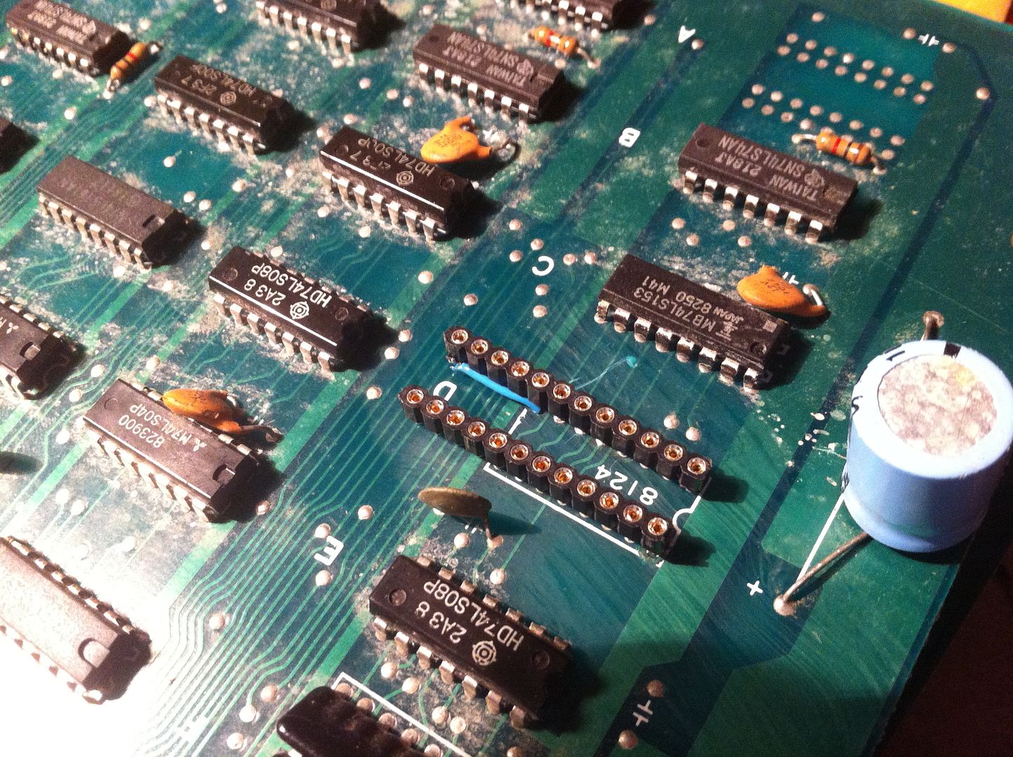
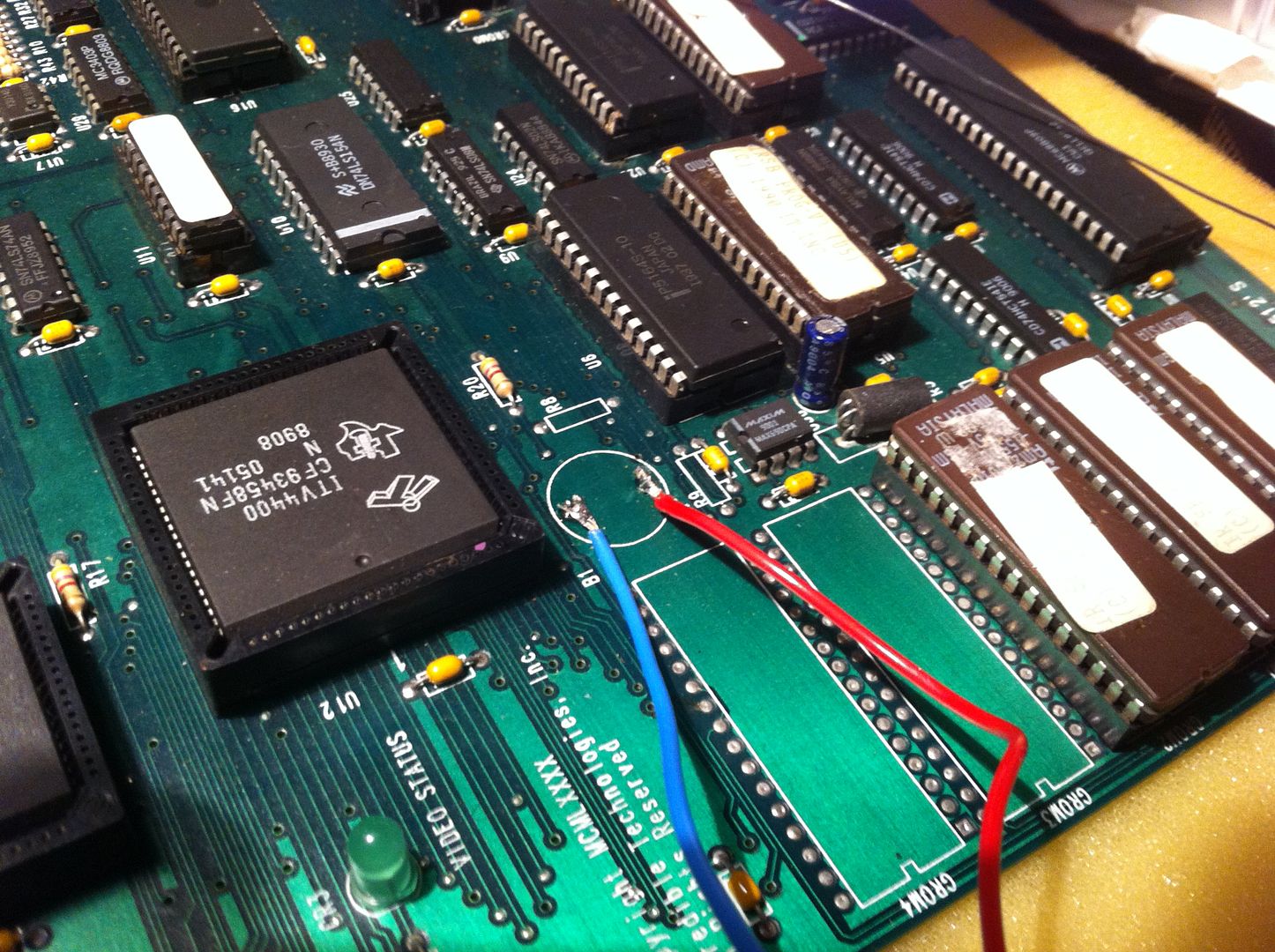
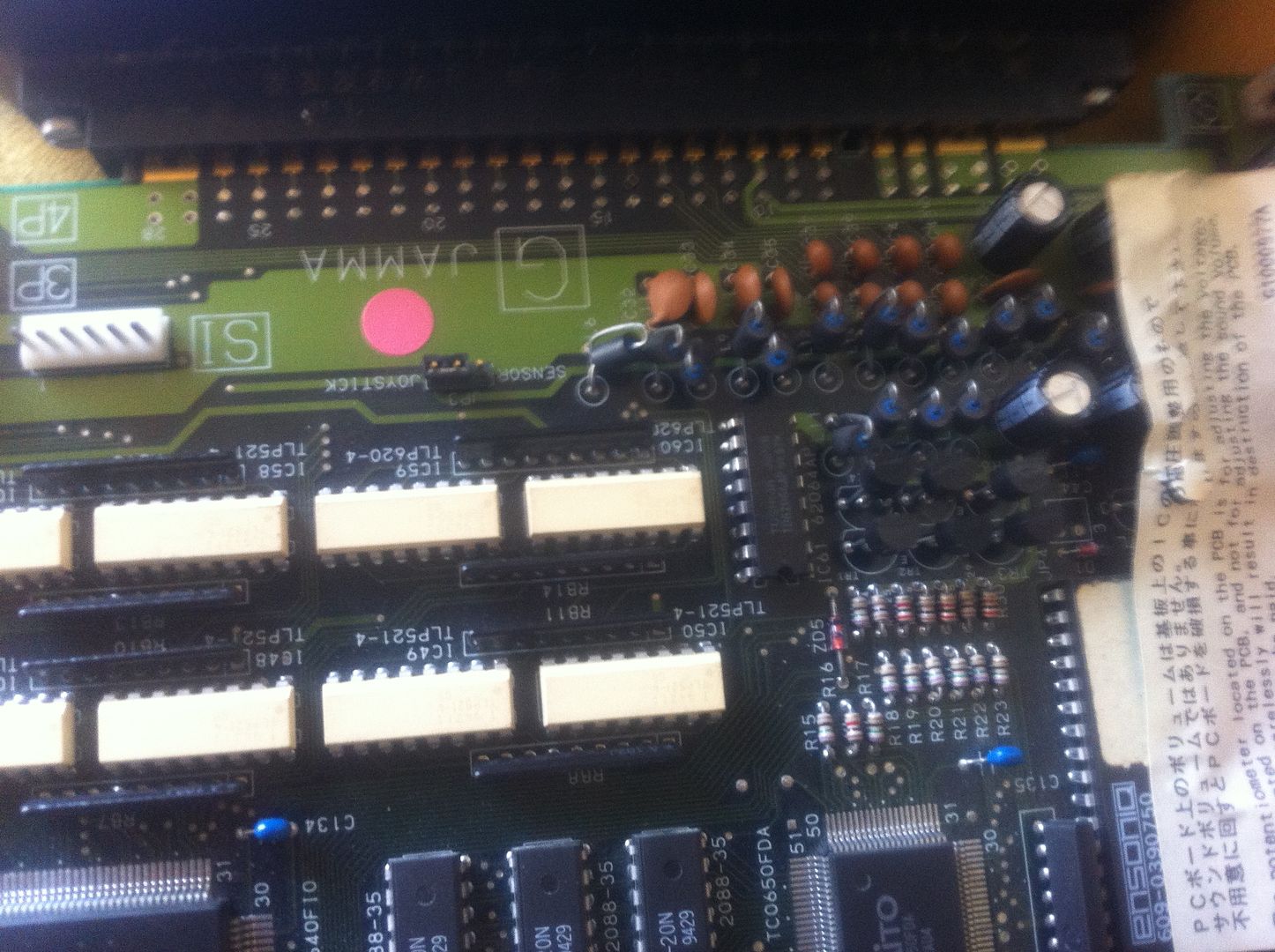
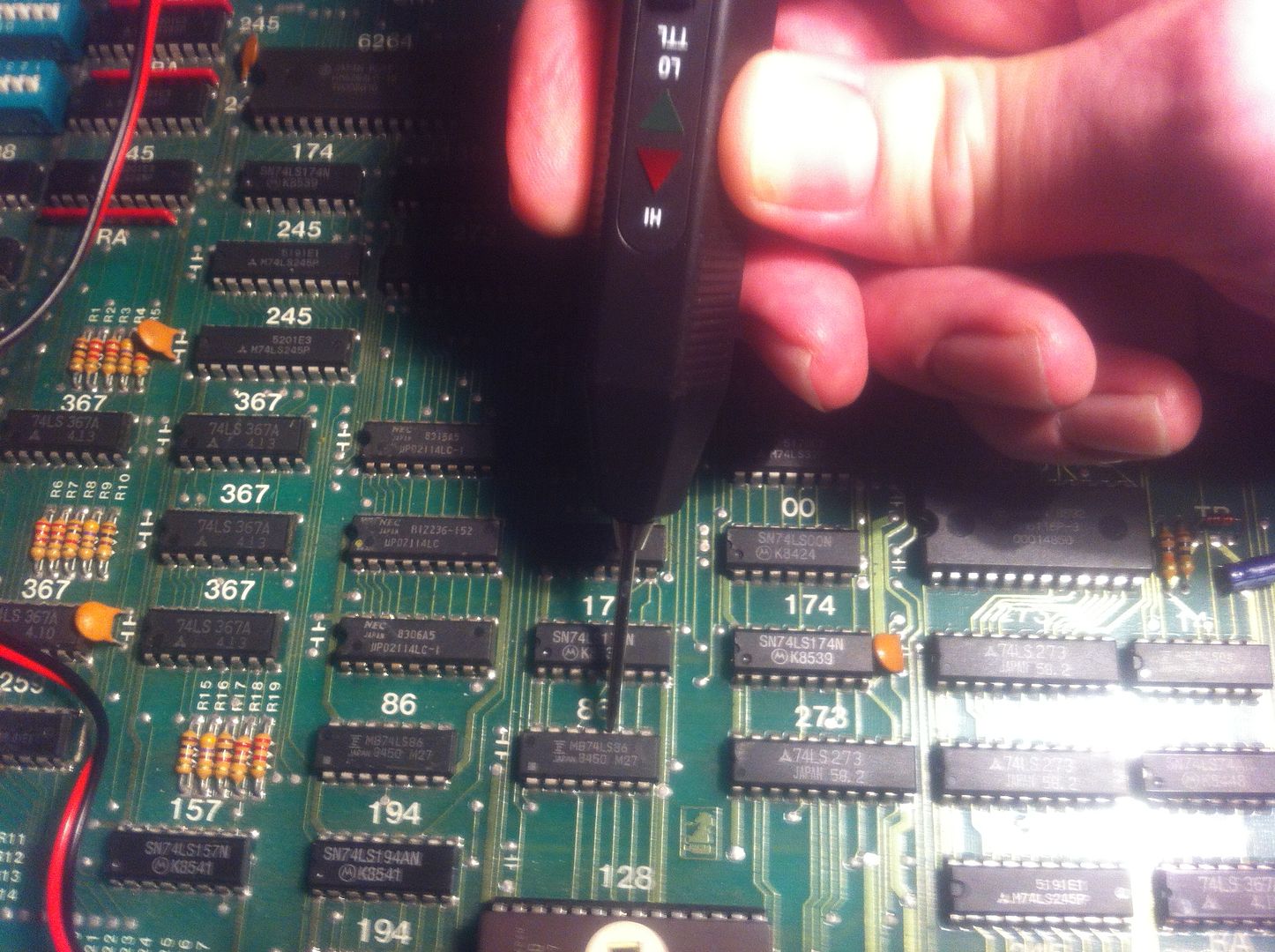
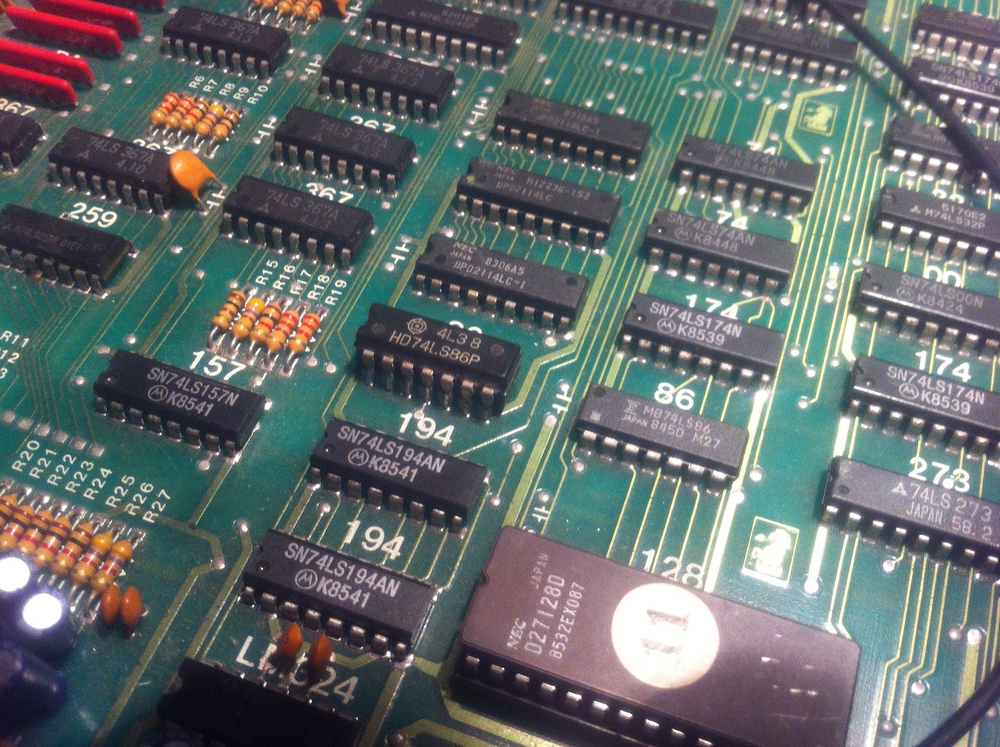
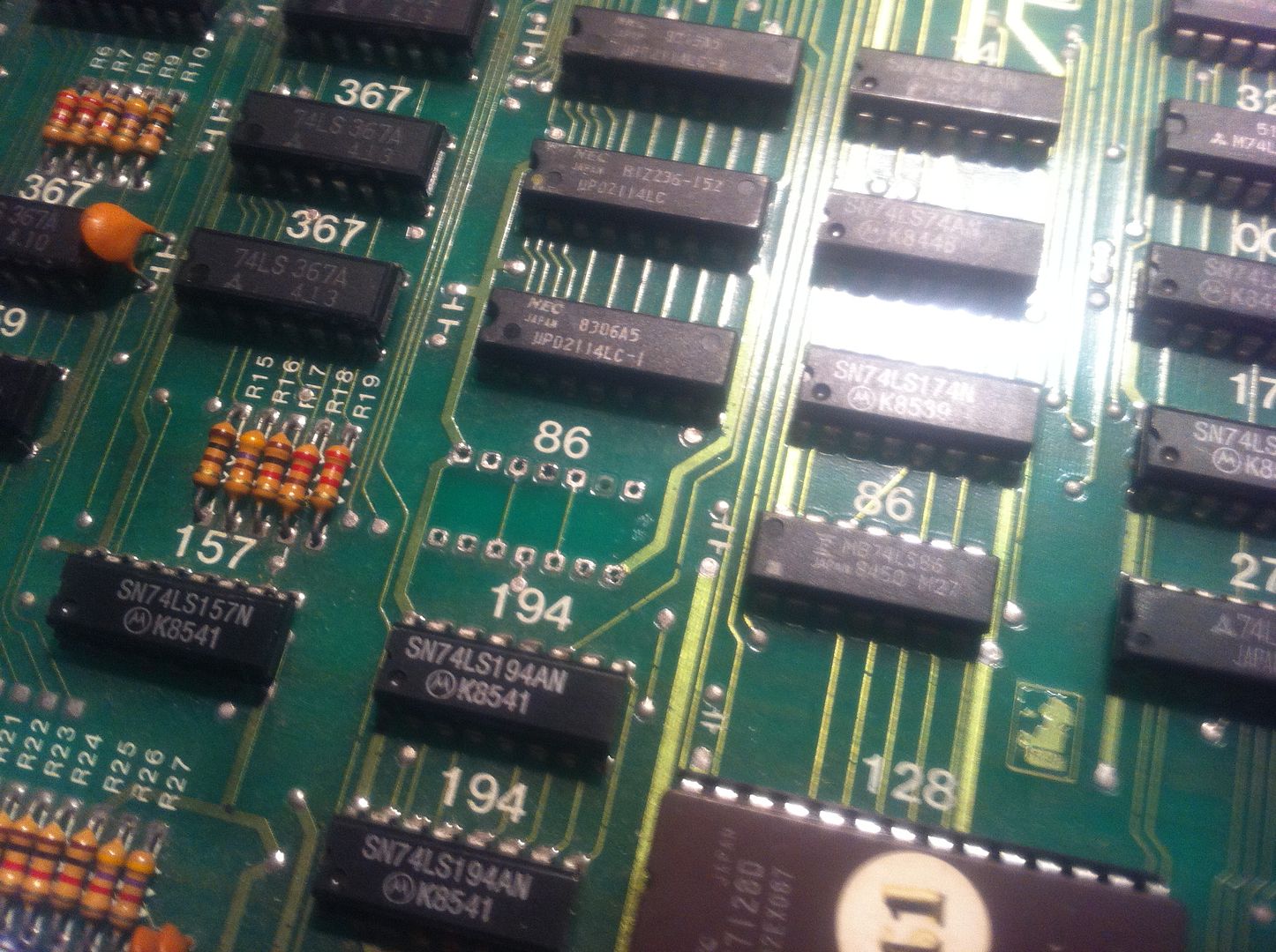
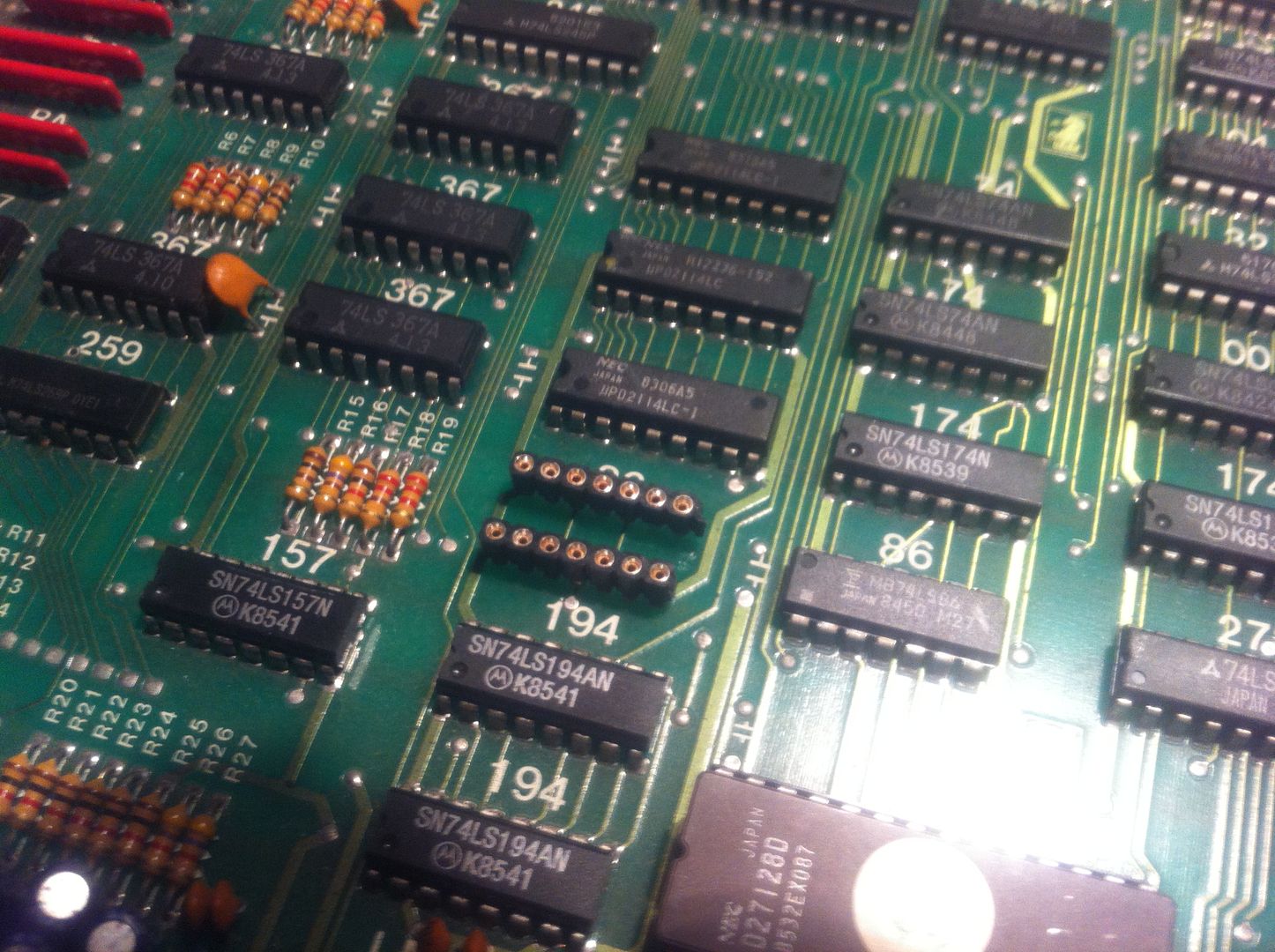
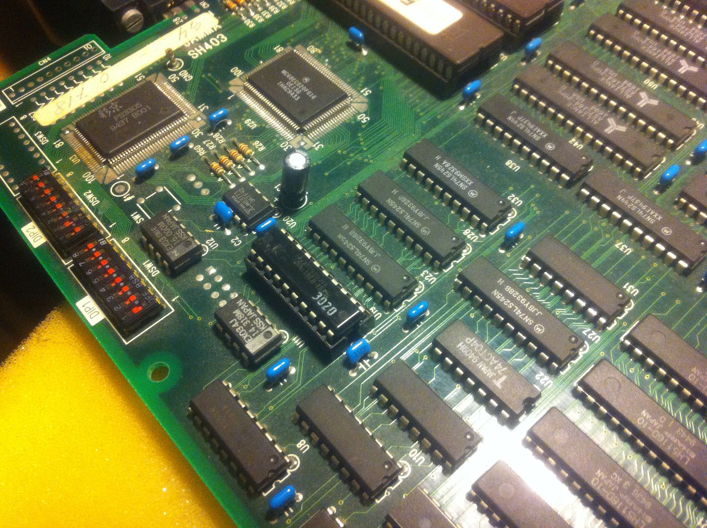
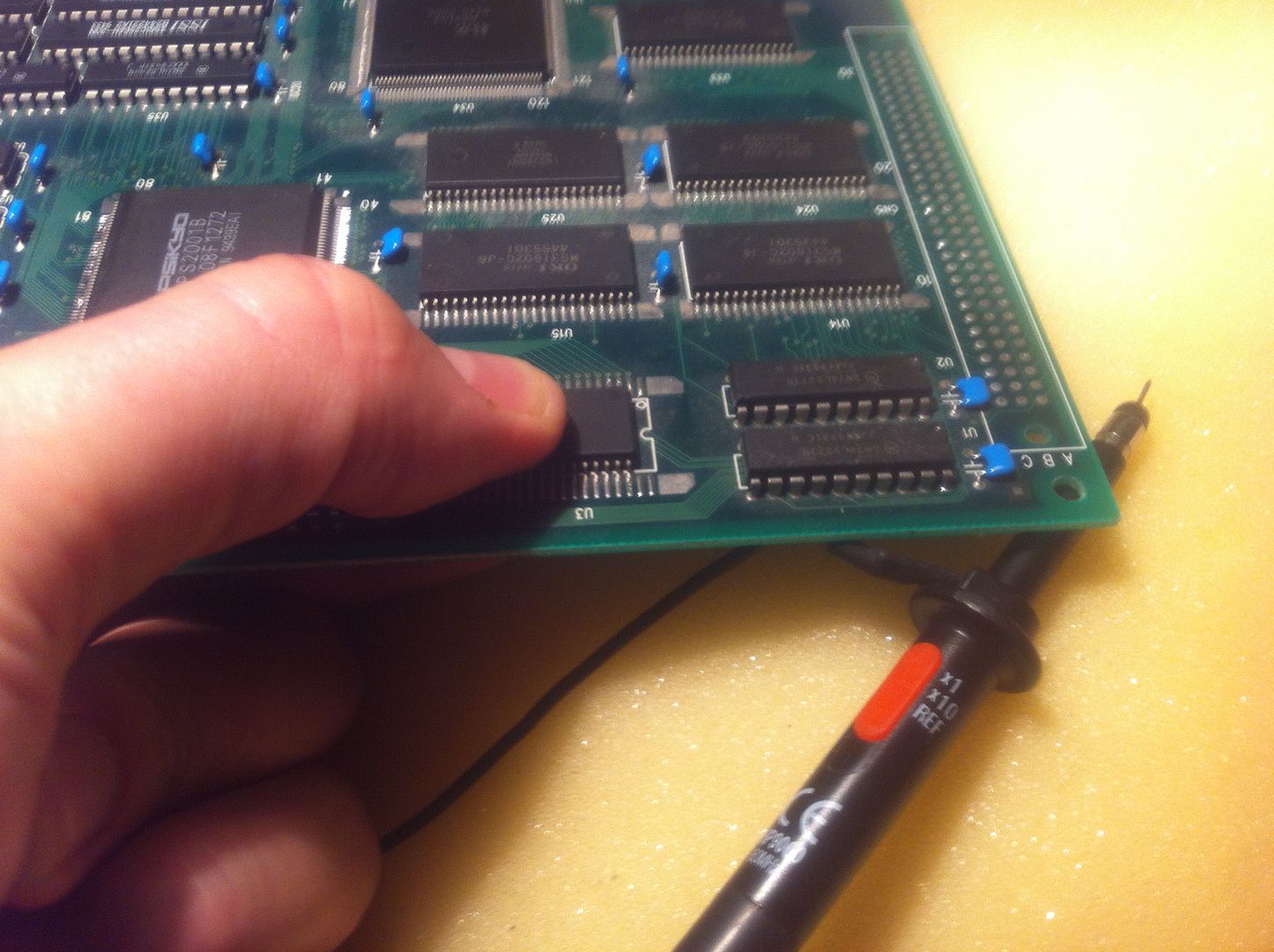
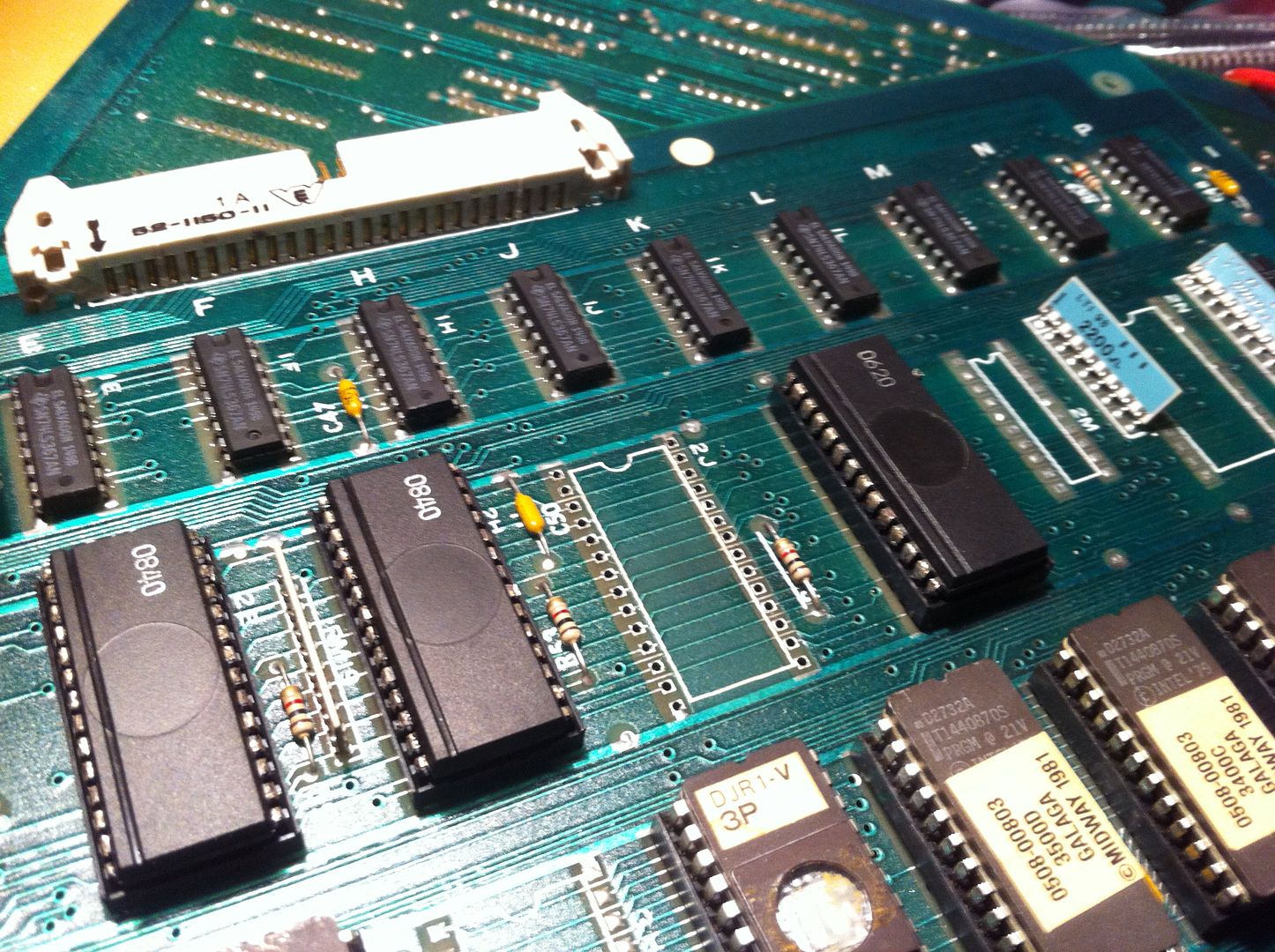
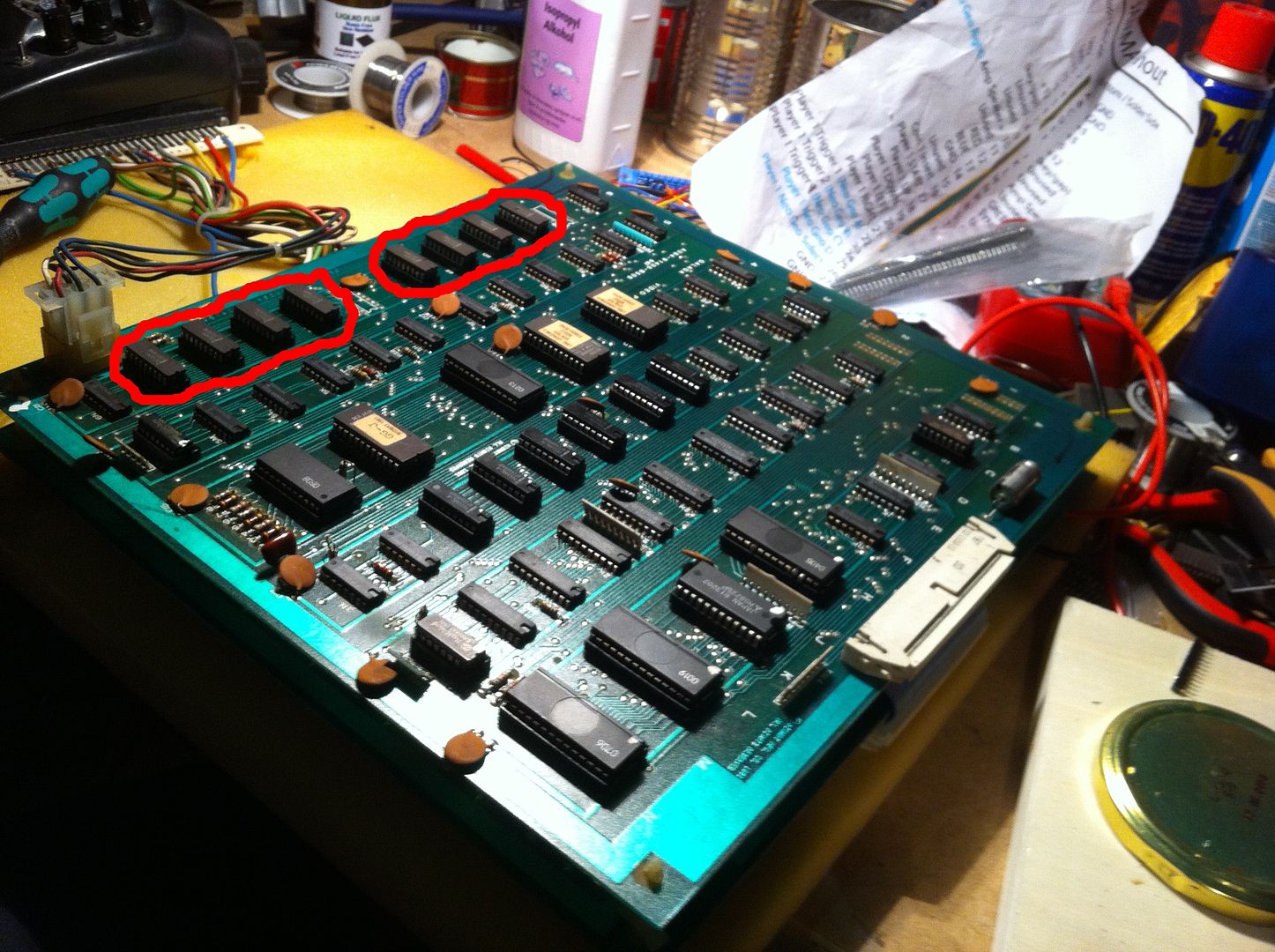
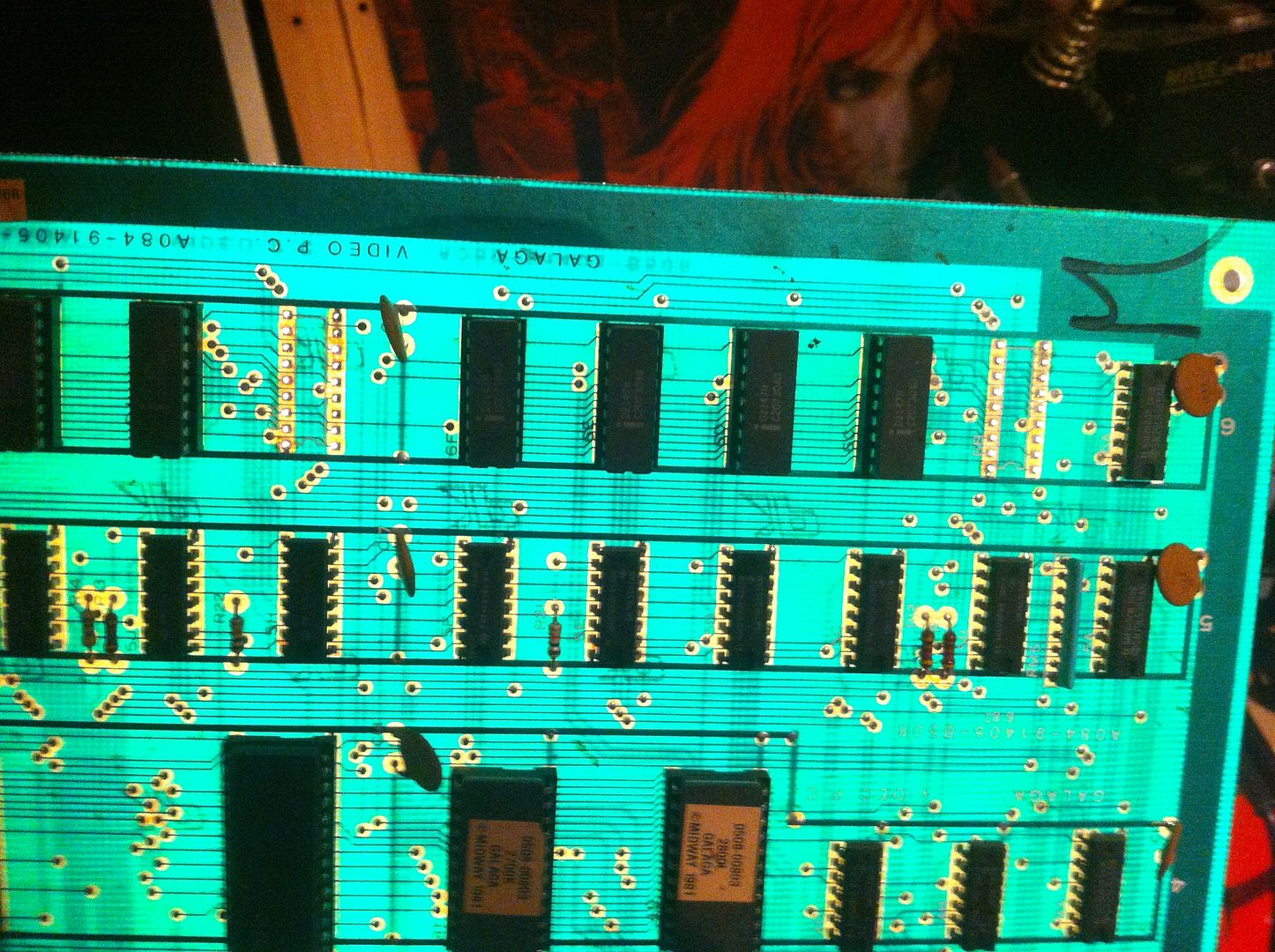
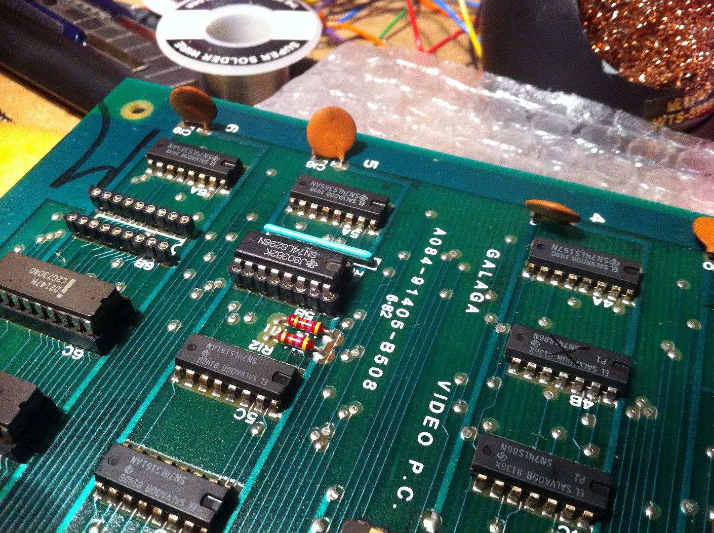
Well on the bright side, it was now time for some REAL hardware debugging instead of just doing clean-up };-P So I dug up the schematics and started scrutinizing it. As i'd already checked all the EPROMs, my first suspect was the sprite RAMs (the 8 ones on the far back of the video board)


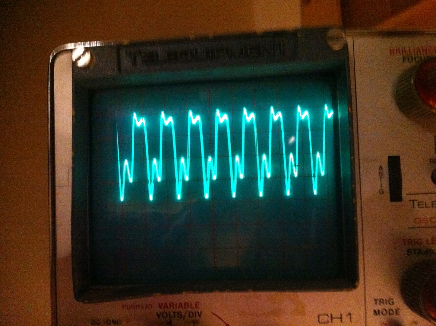
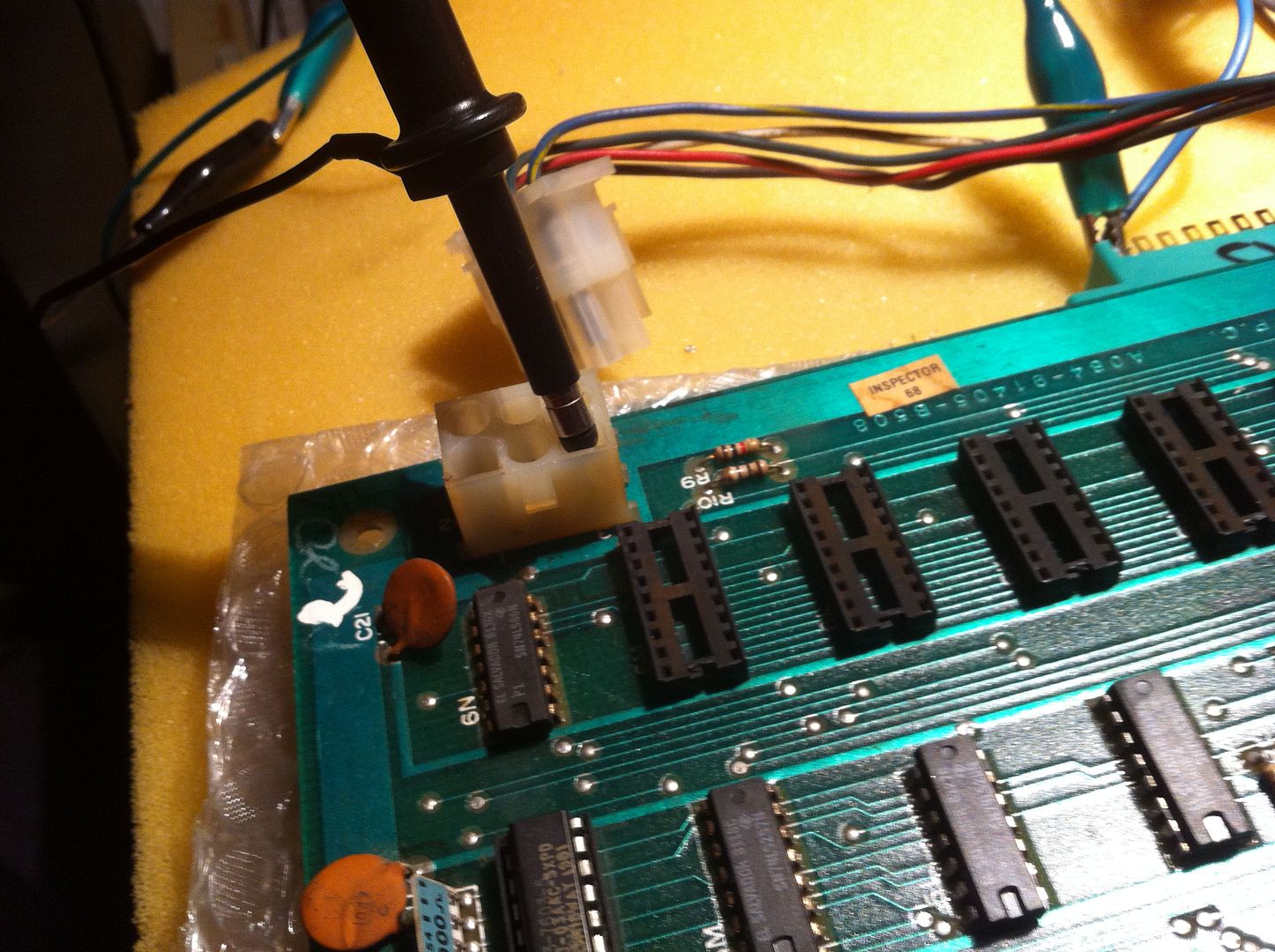
They are 2147 1-bit SRAM in two clusters of 4 (byte wide all in all). So I started hitting them with the scope. But when I touched the data lines with the probe, weird stuff happend on screen


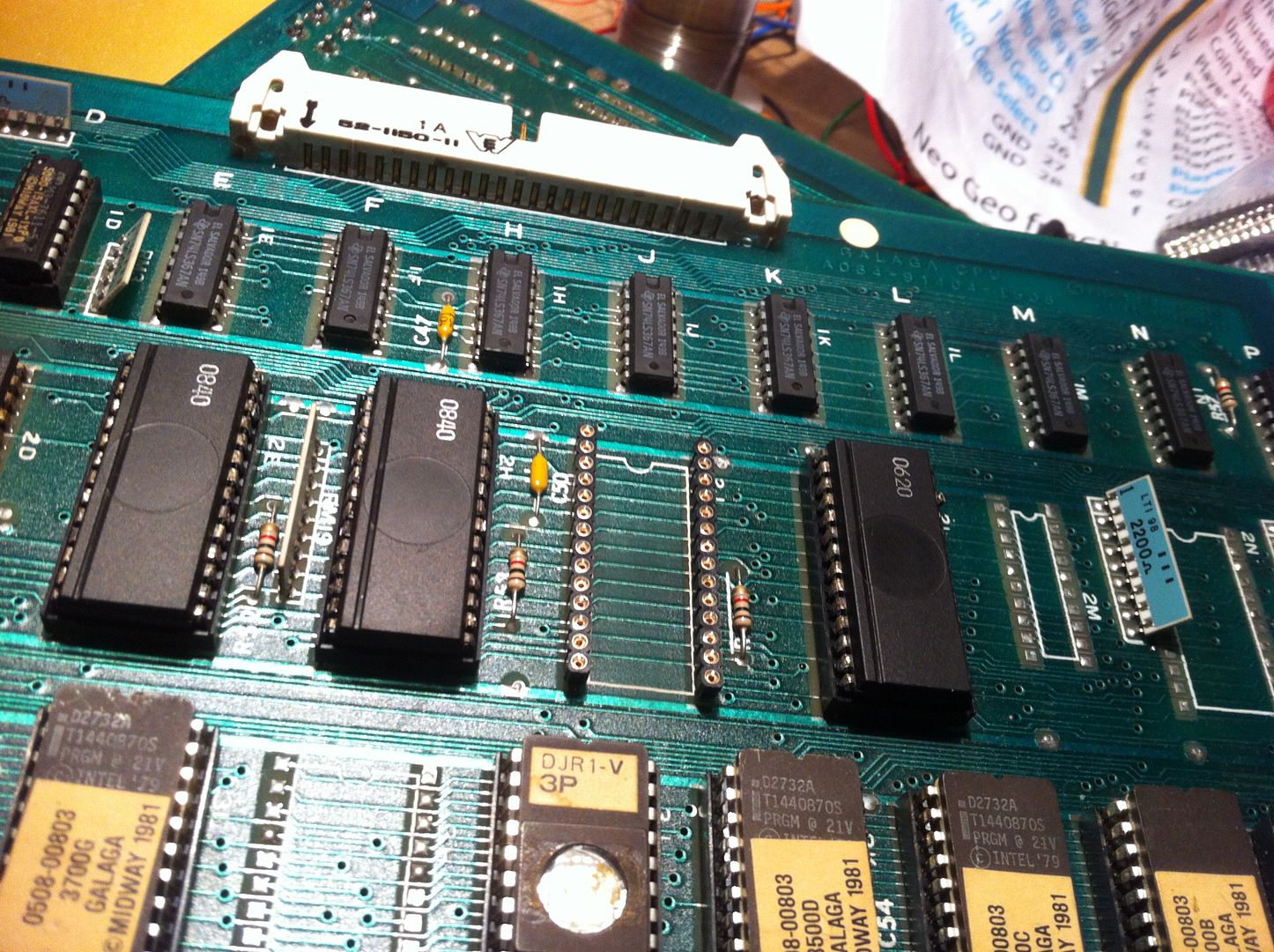
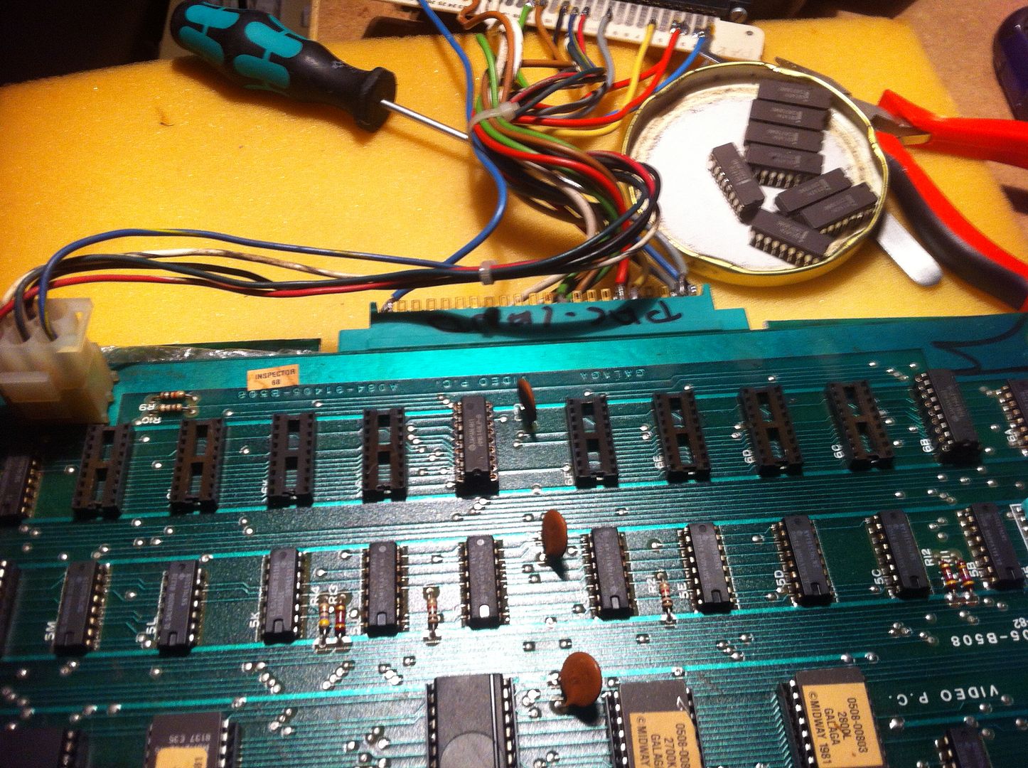
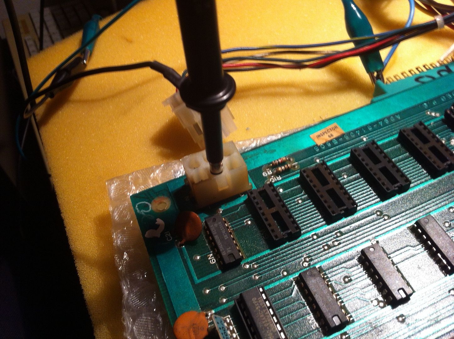
This can be an indication, that something is not driving the lines properly, or the values of the pull-ups might either be too high or too low. Anyway, at this point, I suspected something wrong with the sprite RAMs themselves. I didn't have any 2147 stocked, but looking at the schematics I found, that the video board may be configured in two ways: Either (as this one) with 8 x 2147 or with 2 x 2148 (4 bit SRAMs). This was actually a quite normal thing for manufactures to do back then, as the prices on SRAM were relatively high and also fluctuating. So this way they could wait until the last minute to decide on which to use, thereby keeping the cost of components at a minimum. I did actutually have 2 x 2148 SRAMs on a scrap board, so I harvested these, cleaned the solder holes


fitted sockets and the harvested 2148s, and popped out the 2147s


But alas (ear wax), when I fired up the board, the screen looked precisely the same };-/ Now it would be a very strange coincidence, if the old 8 x 2147 RAMs clustered together, should show precisely the same error on screen as the 2 x 2148. So I assumed, that sprite RAMs were ok. Hmmm, well back to reading them schematics


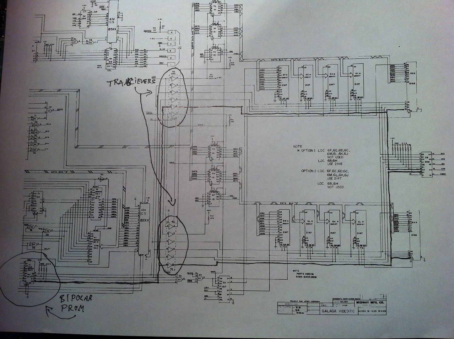
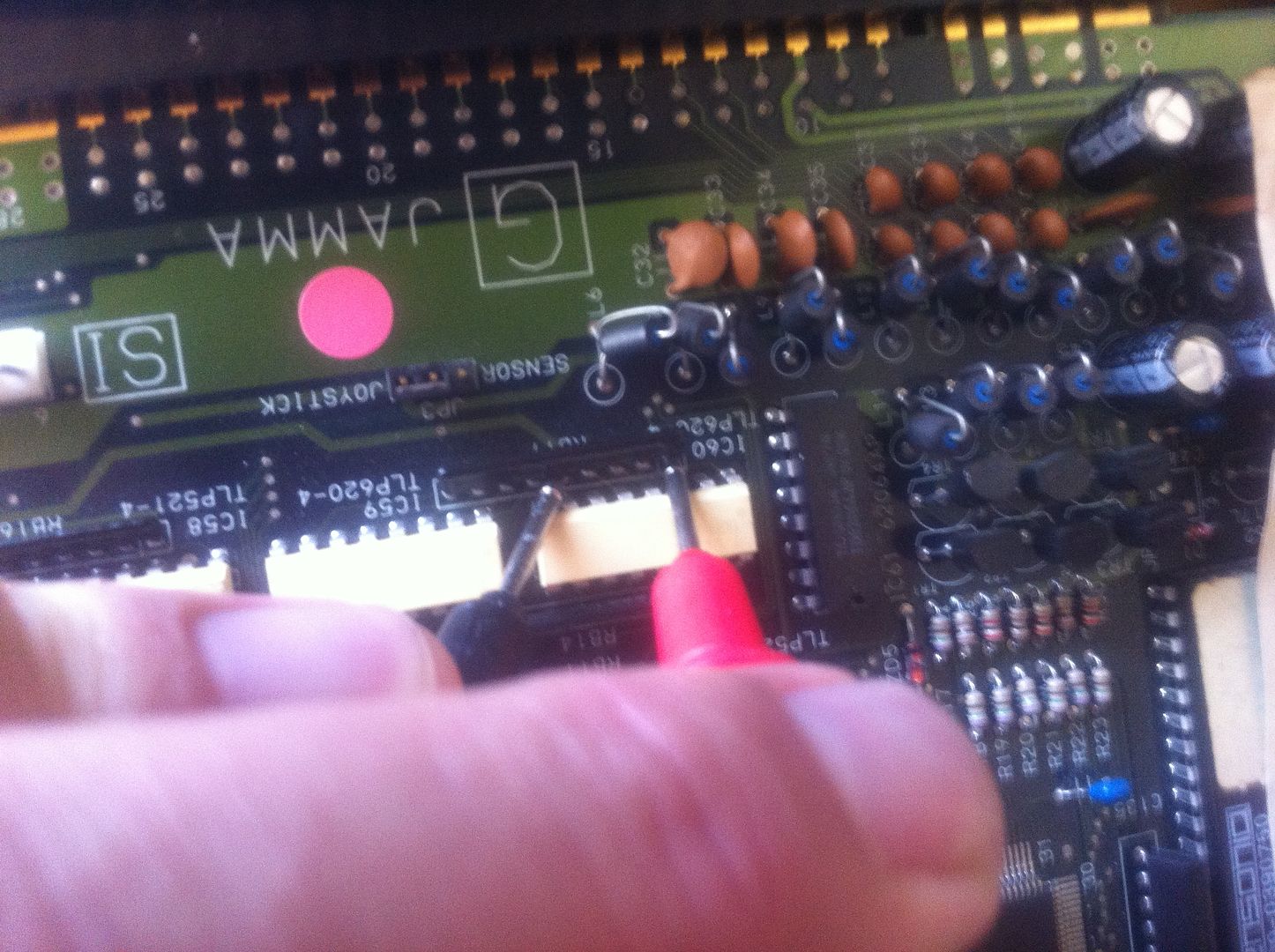
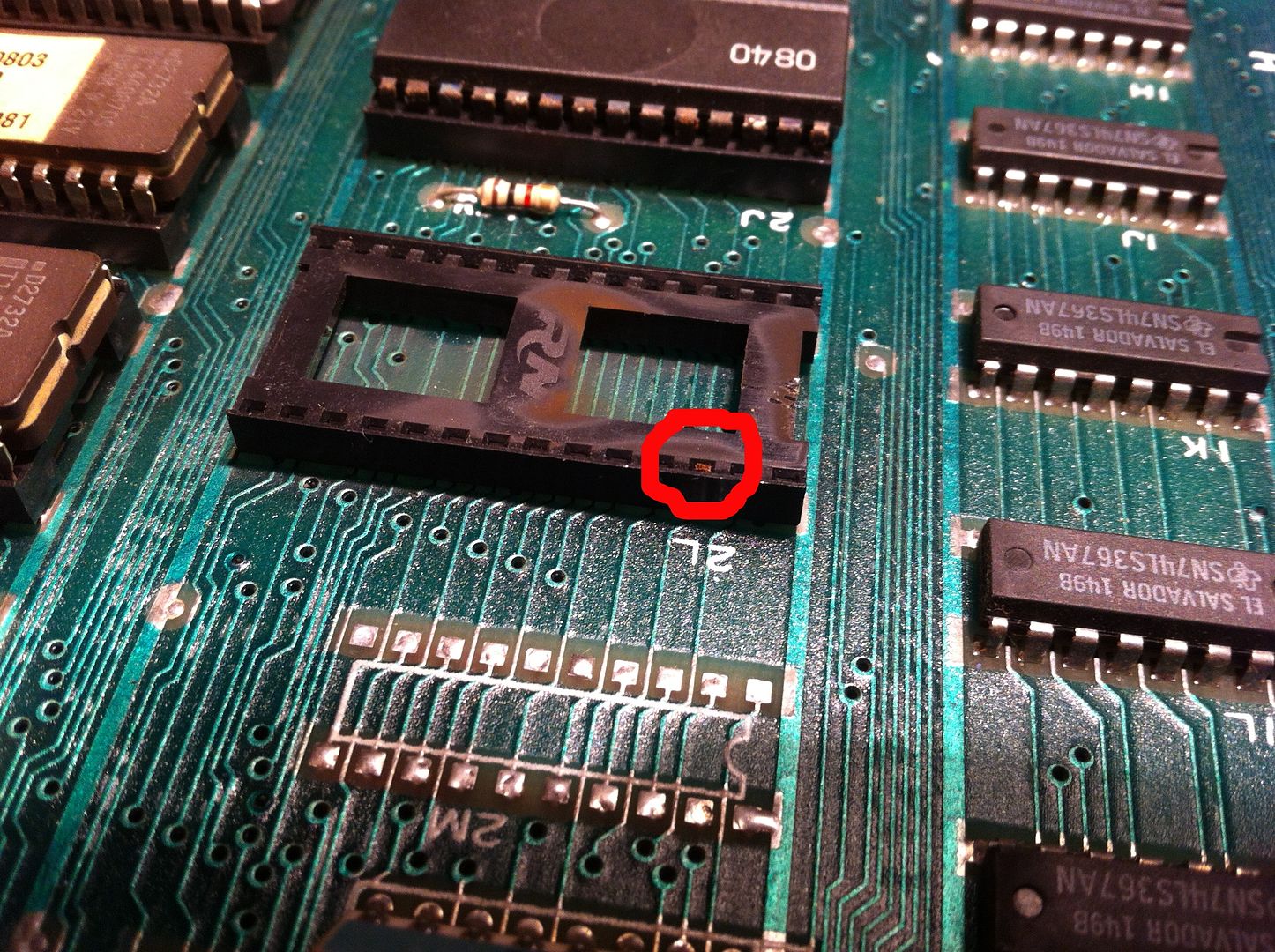
Also on these datalines is the Namco custom IC that generates the actual sprites by mixing the signals from the data lines placed on the far right on the picture above. However, if that was broken, I'd be frakked anyway, so I assumed, that it was ok too. The last things directly on these lines, was the 2 transceivers in the middle of the picture (marked with 2 circles). When peeking the lines on the topmost of these, I discovered, that one of them was stuck high.


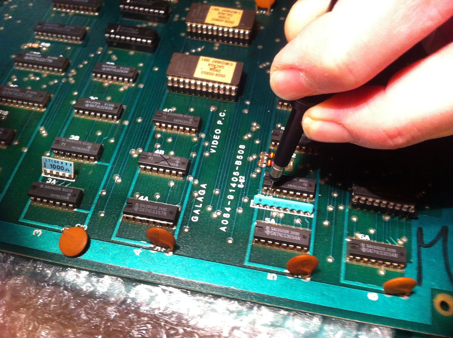
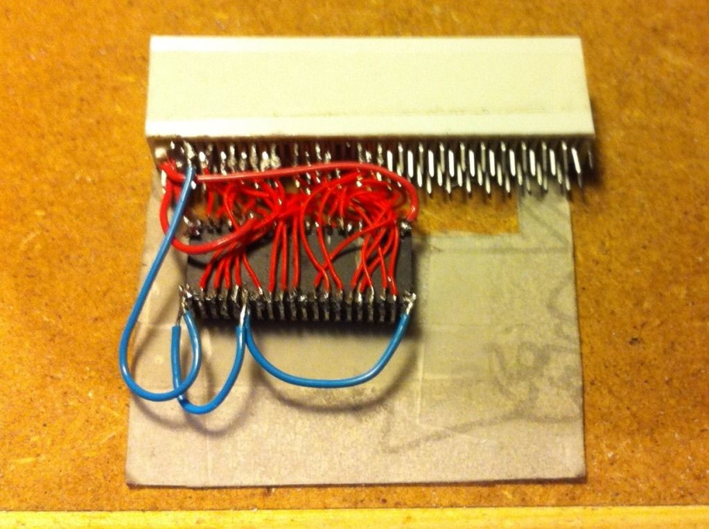
The input seemed to be active, so desoldered the 298 TTL, but in my eager accidentally broke a couple of pins. However, I was determined to get it tested in the Top, so I quikly fitted some header strips as new pins. But it tested good in the Top


So fitted the pathed-up 298 again, as I was "in da zone" and just wanted to move on...


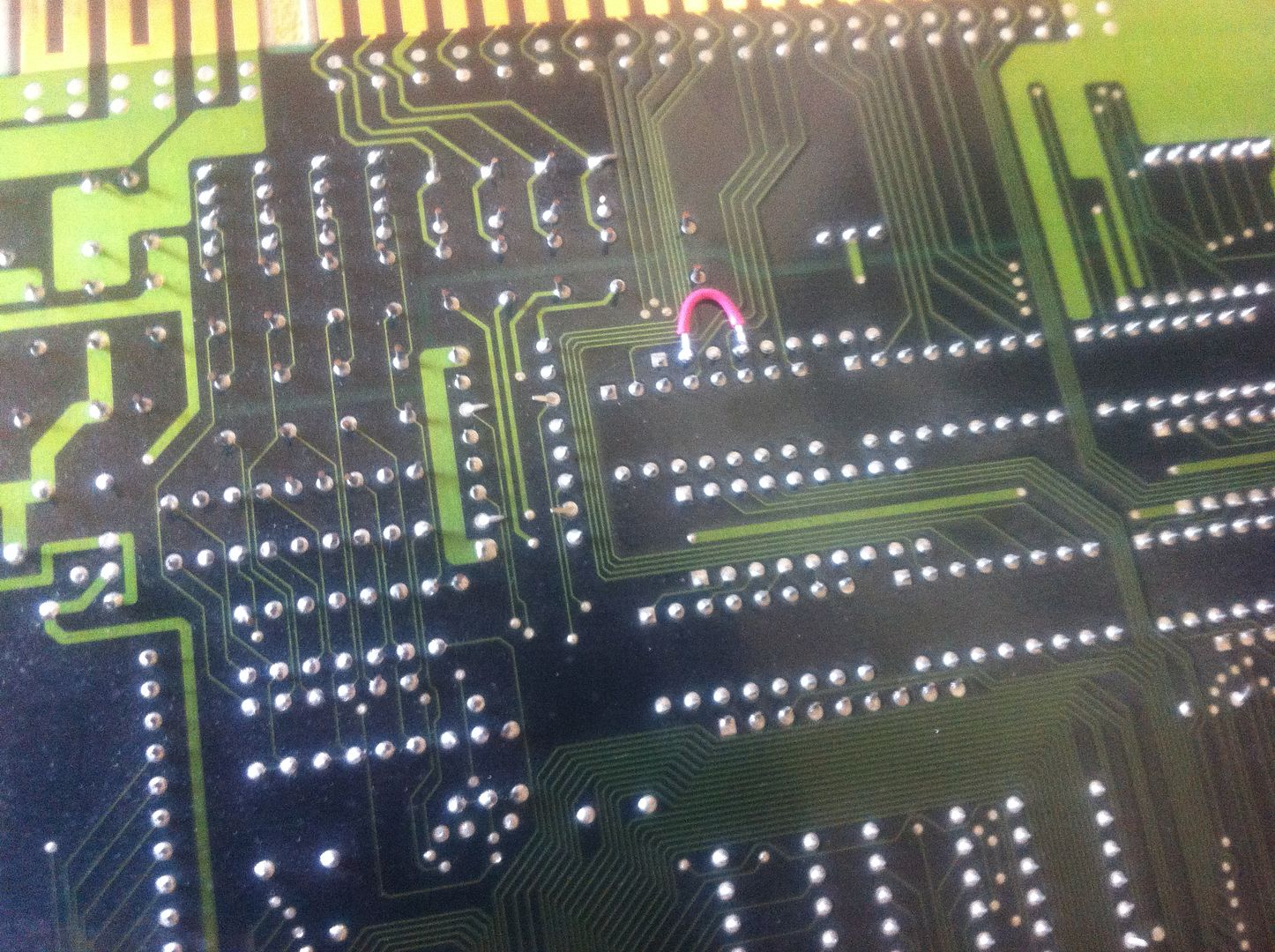
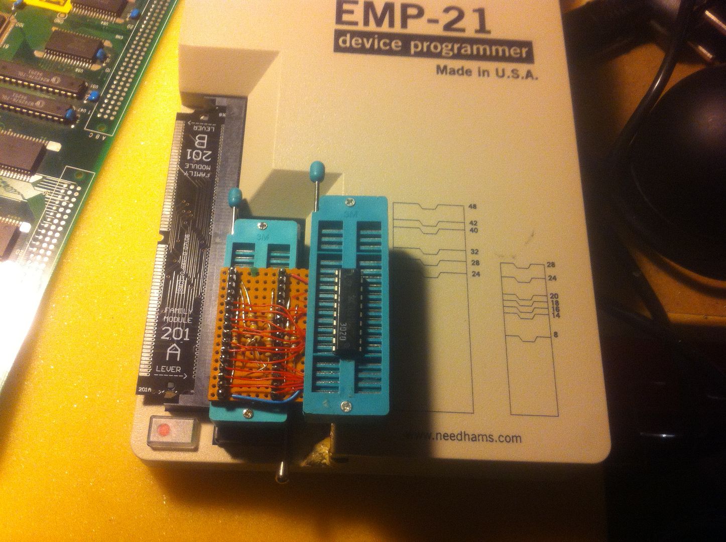
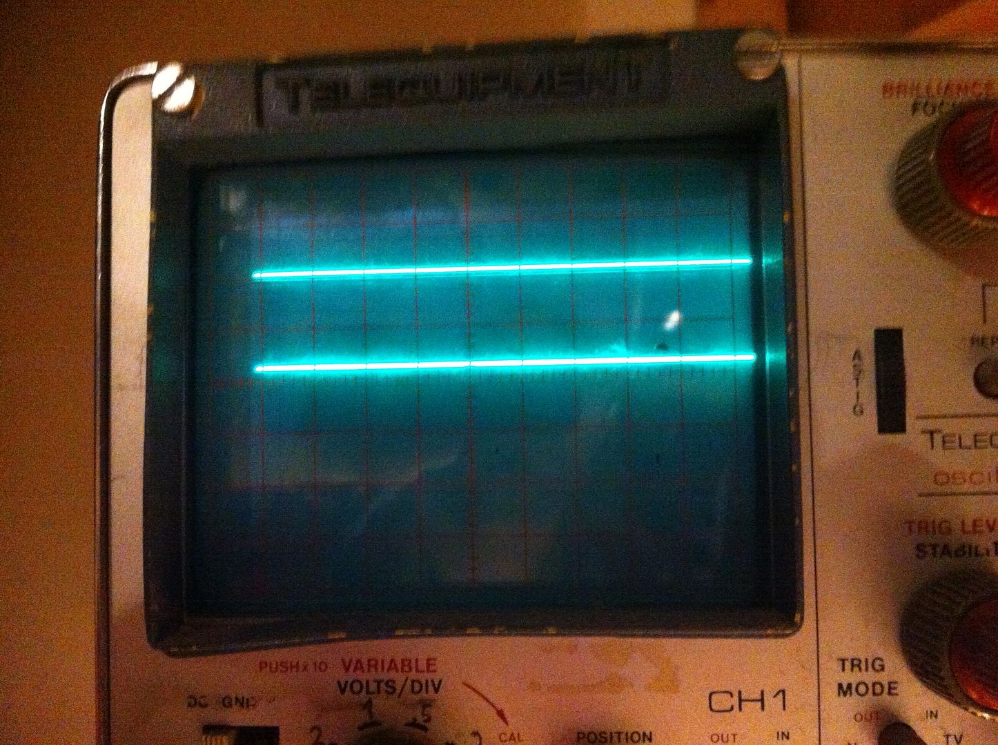
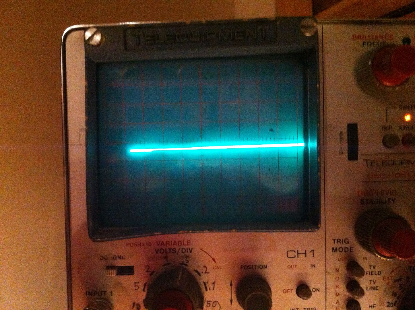
Hmmm, the signal on the input of the stuck line still looked more-or-less ok on the scope. But maybe the lows wasn't quite as low as on the other inputs?! (haven't got a picture of this, sadly). At this point, my new Logic Probe (with audio feedback) had arrived in the mail, and I decided to test it, as sometimes it can be had to see on a scope, if the signals actually reaches the logical thresholds. As one can see, the only thing connected to the inputs, are the outputs from the bipolar prom in the lower left corner of the schematics picture. So lifted the suspect pin along with one other out of the socket, and hit them with the probe. First the suspect


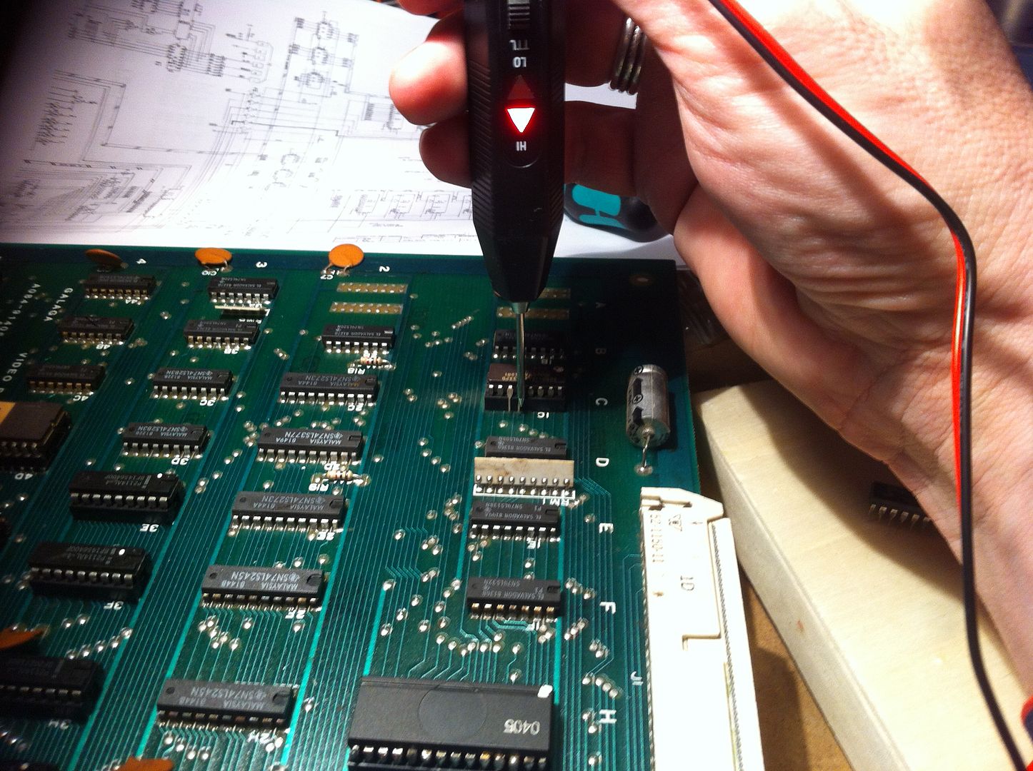
and then the assumed good


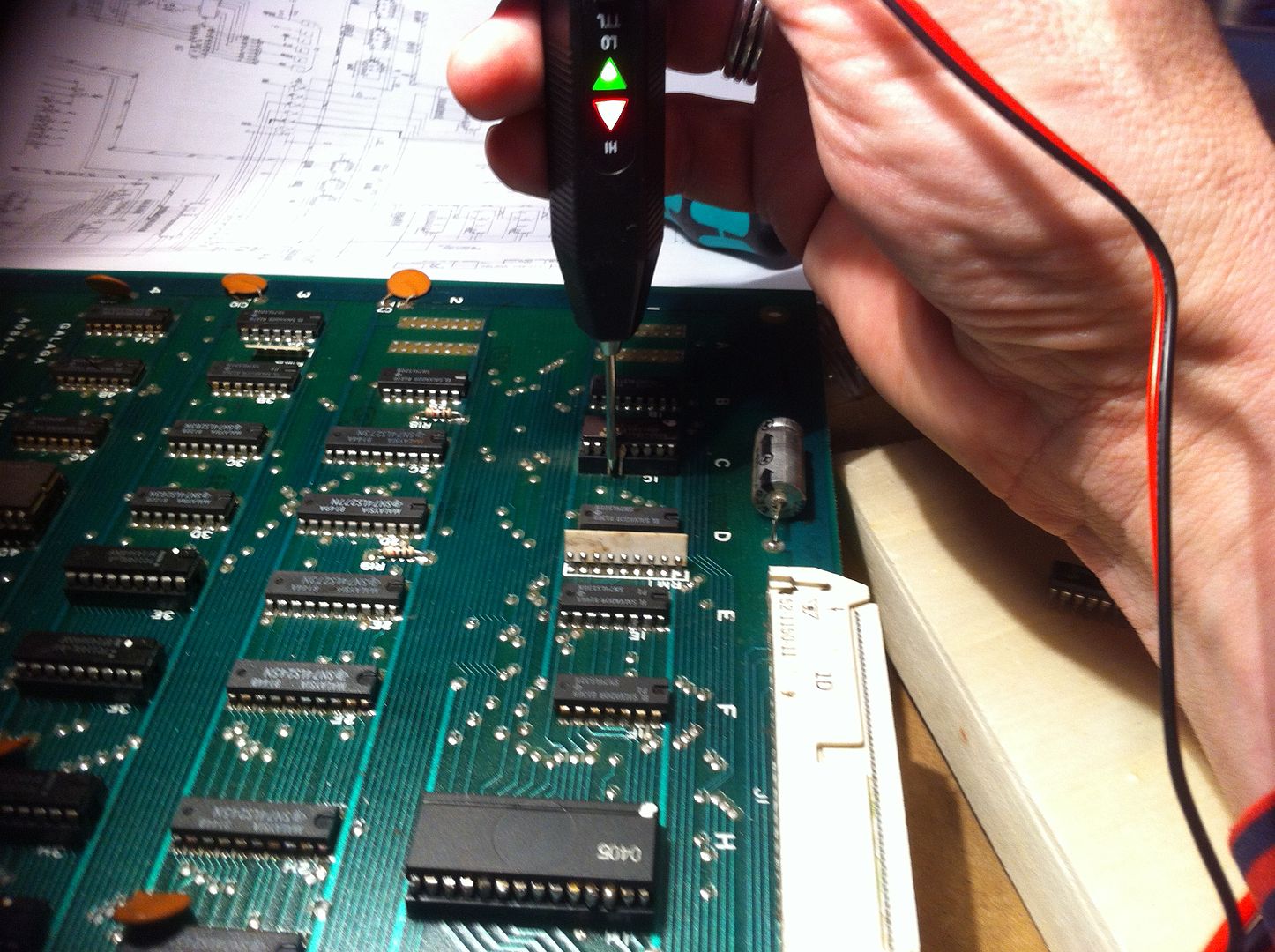
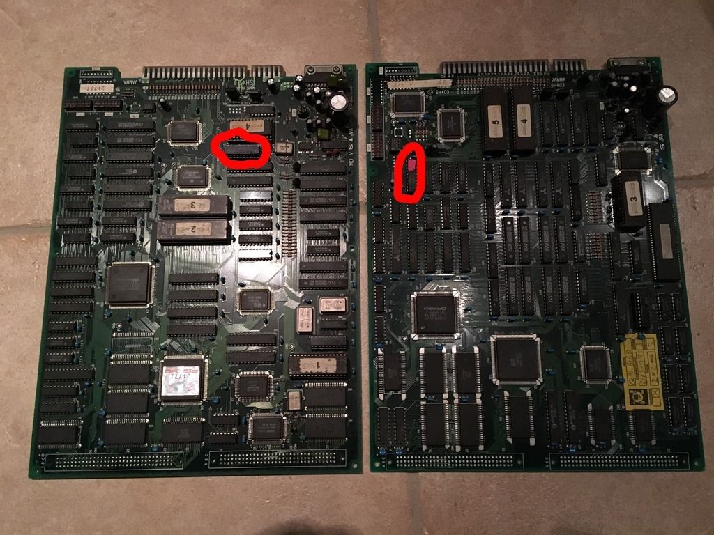
Now of cause, as the pins were now out of the socket, they were not pulled by the pull-ups. But as this pin was stuck HIGH (and not low), that couldn't explain what I saw. To be sure, I peeked the inputs to the PROM, and they were all active. I'd finally found a culprit! };-P However, I don't have any readers that can read/write bipolar PROMs, so what now? I then remembered, that I had a working bootleg Galaga on the shelf. So I found the corresponding place on the bootleg


and compared it to the original


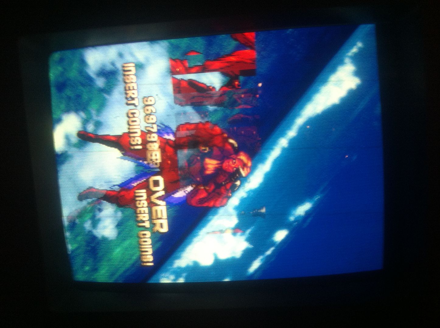
It looked almost identical, and the ICs on either sides of the PROM (marked "5" on the bootleg) was the same. I googled the pinout for TBP24S10N and found it to be the same same as on the original schematics. So I slammed the bootleg PROM into the original Galaga, aaaaand... PRESTO!


The kidnappers looked normal, even when floating at the top of the screen. So I fitted a 298 harvested from a scrap board for the patched up one, to close this up nicely.


Now I was down to, that the only thing wrong with this game, was the overall purple-ish look of the screen. So I disconnected the video plug, and peeked the colour signals


From the last pictures, it was obvious that one of them was dead. Looking at the solder side, I was relieved, as I found that the trace was broken just before the solder patch (the middle one)


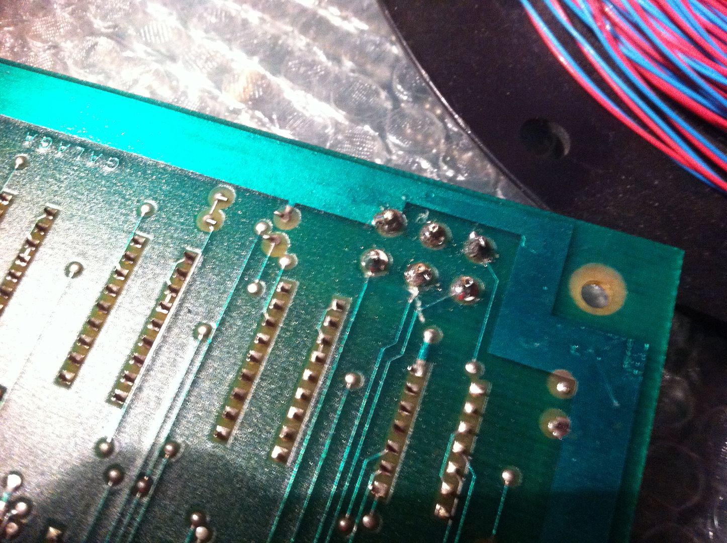
As the one on the rigth in the picture looked like it could snap at any time too


I patched both for good measure, and all the colours was now clear and crisp. So now the game was all good to go, PEW! };-P

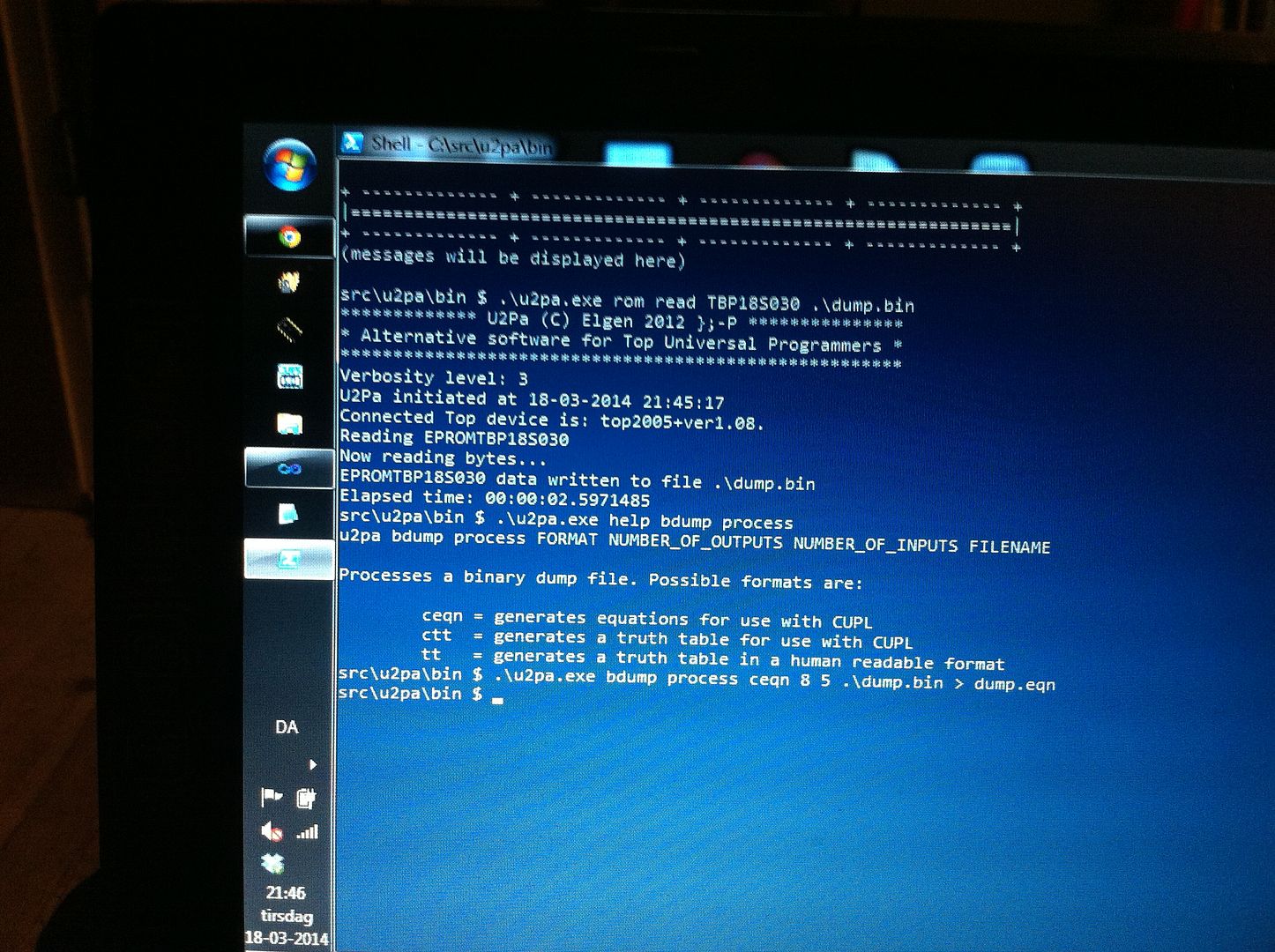
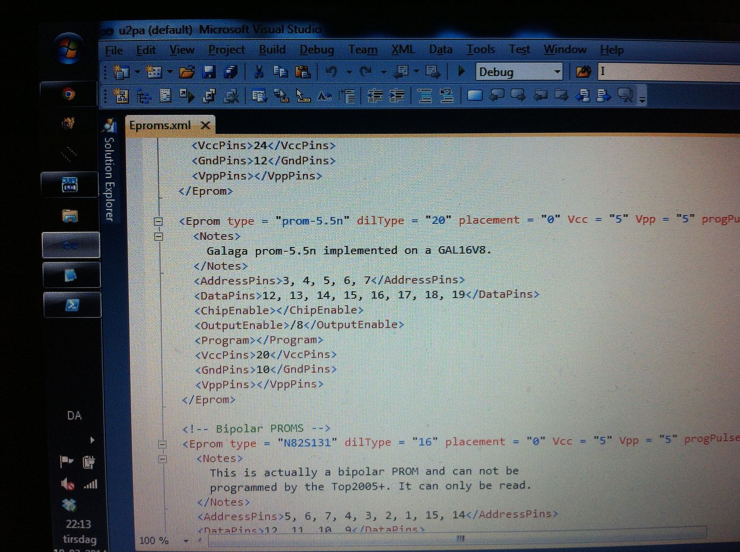
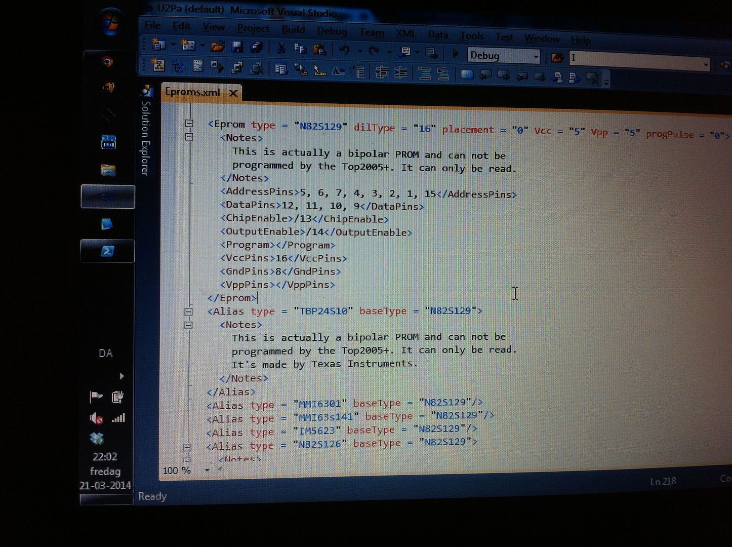
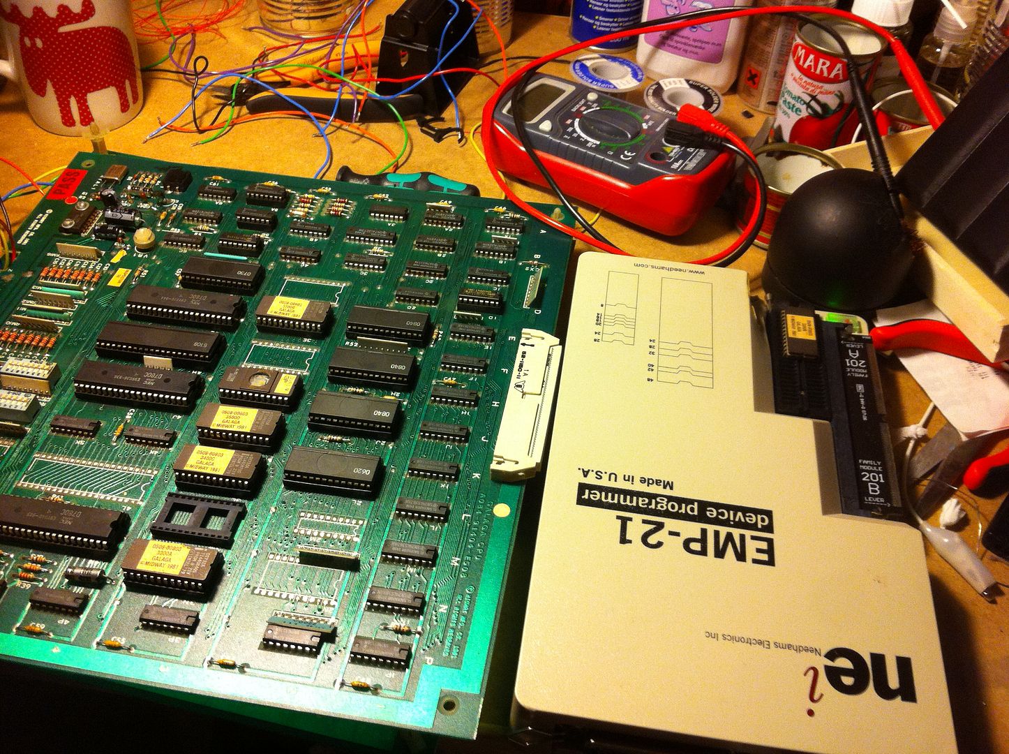
Now what about the poor working bootleg that he harvested the bipolar PROM from, you might think?! Oh, well it wouldn't be Elgen, if he didn't have a crazy idea for a future project, would it? So I made some minor changes to u2pa (my own GPL sofware for the cheap Top2005+ Programmer) enabling it to read the 2 types of bipolar PROMs used on Galaga, so I would be able to test them against MAME in the future. I actually also tested the one that I used for the original, to be sure it's the same as the dump in MAME, and it is };-P I now began thinking, if I maybe could use some other programmable device that my equipment can handle in place of the PROM; even though I was now able to read the bipolar PROMs, programming them is a whole different ball game. The first thing that popped into mind, was using an EPROM, but they are far too slow; about a factor 10 slower access time than bipolar PROMs. Then I thought about using a GAL, but at this is a logical device, the PROM dump would have to fit into a truth table for it to be doable. I now contacted my dear friend porchy, who is far more experienced into the world of GALs than me. After having had a glance at the dump file and the Galaga schematics, his verdict was that it might very well be doable. Cool };-P So I made a small QAD command line tool, that generates (unreduced) equations that can be used in CUPL from a dump of a bipolar PROM; it's included in the u2pa package (if your not friendly with hg, a current snapshot of the repo can be found here, if you're interested in having a look at it). I haven't come any further at this point, as I have some other repairs queued up. But I'll definitely look into it in the future };-P

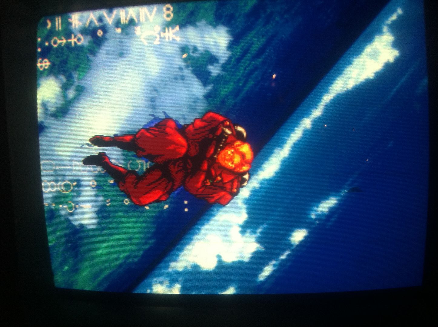
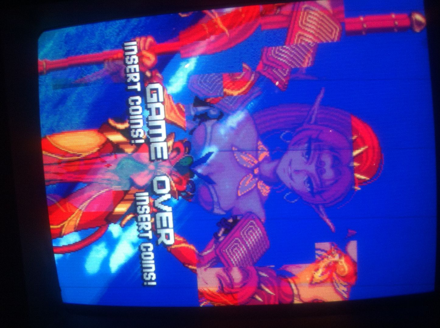
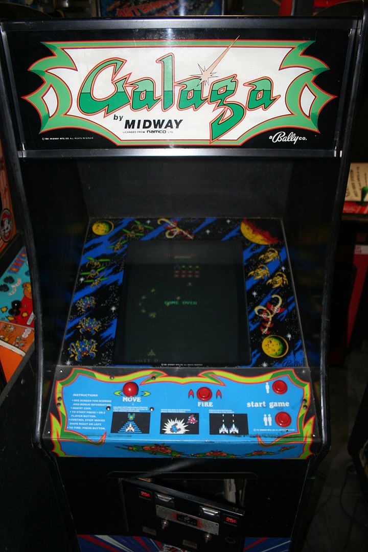
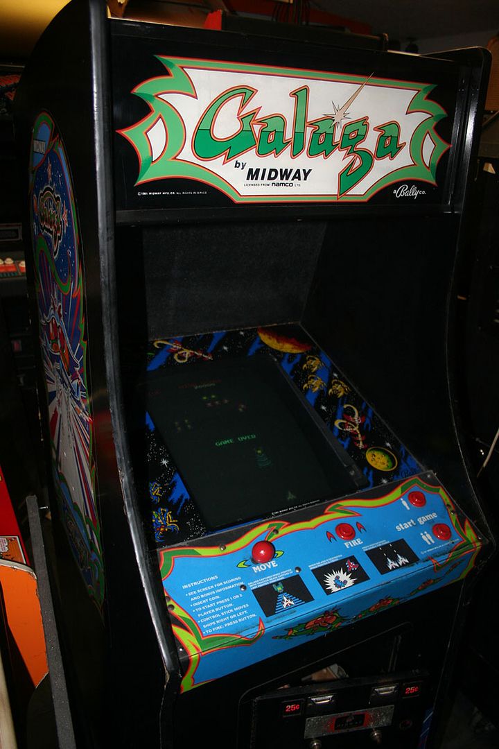
After Muerto recieved the game, he sent me these nice pictures and YouTube-links of it running in his original dedicated Bally Midway cab. Enjoy! };-P


Last but not least, Muerto was so thrilled with his Galaga now finally in working condition, that he made this totally awesome poster of me.

 It's a poster! I like posters. Posters are cool!
...just like bow ties, fezzes, and stetsons of cause };-P

Using GALs to replace small, sparse and/or redundant bipolar PROMs (Galaga bootleg)

$
0
0
If you've done repairs on some of the earlier arcade games (Galaga, Donkey Kong, Pac-Land etc.), you're likely to have encountered the type of components known as bipolar PROMs. These are PROMs based on TTL technology and are one-time-programmable (OTP), as you literally burn fuses when you program them. They are often pretty small in capacity but very fast, and on many boards, they are used for things like address decoding, sprite selection, pallets etc.
Now this whole project started out with me repairing an original Namco/Bally Midway Galaga for my friend Muerto. During this, I found, that a bipolar PROM used for selecting sprites from the sprite-ROMs (i think?!) had a dead pin. Luckily, I had a bootleg Galaga containing the same PROM sitting on the shelf, and replacing with that solved the problem. But now I just a non-working bootleg.
Now as bipolar PROMs are pretty old technology, blank ones are not easy and also a bit expensive to acquire; they will easily cost you $10 (or more) a piece + P&P on eBay. Also because of the technology being old, most new (even high end) programmers doesn't support programming them either; many doesn't even support reading them. So that means that you'll have to get some expensive hard-to-get vintage programmer and also expensive parts to get you PCB with broken bipolar PROMs up'n'running again. As I was not willing to spend that much green on a bootleg (that I btw had gotten for free at some point), I started thinking about alternatives to bipolar PROMs.
The first thing the pops into mind, is trying to use some kind of EPROM. But when you try to look at the specs side by side, you'll quickly realize, that most EPROMs are much bigger in capacity (and while that is not a direct problem, it seems like a bit of a waste), but more seriously, the speeds of EPROMs are often about a factor 10 slower than the bipolar PROMs! So EPROMs were out...
Next I started looking at different PLDs and found, that the speeds of standard PALs and GALs are often comparable to that of bipolar PROMs or a bit faster. Moreover, almost any cheap ass modern universal programmer supports programming GALs, you can get new GALs for about $1 a piece on eBay, and you can erase them electronically and reprogram them.

I actually had 2 defective bipolar PROMs on the bootleg Galaga, that needed replacing. That was because when I realized how easy it was to read these in my Top2005+ using my own software u2pa, I wanted to


on the Galaga PCB. But when I tried to get the one labeled "5" at position 5N out, I accidentally broke off the GND-pin. The break was so near the plastic, that a normal pin transplant wasn't an option, so enter Mr. Dremel. I managed to cut the plastic down so I could solder a bit of wire on the broken pin; it was good enough for dumping


but not at all durable enough to put back in the socket. This PROM must be involved in the final stages of the picture generation, cause when it's not in it's socket, all you get is a blank screen. I decided to start with that one, as it's a TI TBP18S030 (equivalent to the better known Philips N82S123),


that only holds 32 bytes (= 256 bits).
Now in order to get started, I needed some way to generate the equivalent equations, so I wrote a little QAD method that generated the Boolean equations in the format of WinCUPL, and hooked it up to the u2paCLI


If we start by looking at the raw dump


we'll see, that the 2 lines of bytes, are actually pretty redundant, and that's good, as we want to fit then into a logic unit. Next we take the raw WinCUPL equations generated by u2pa


cut them out, and make them into a real WinCUPL project. And I have to admit, that I was a bit surprised to find, that it compiled to a GAL16V8 right away };-P


At this point, the observant reader should already have noticed, that all the outputs of the GAL are on the "wrong" side, compared to the data pins on the bipolar PROM. Some kind of adaptor had to be made in order to make it fit onto the Galaga PCB. I choose this configuration of pins


Again the observant reader might have discovered, that if you turn the GAL 180 degrees, you can get all but one pin to match the PROM (not including the Vcc and Gnd of cause).
When I dumped the GAL using u2pa with the above configuration and compared it to the original


it was a perfect match };-P
So I started soldering up a small adaptor


Actually pretty easy, as almost all the pins match up };-P I dumped it as per the original PROM and still got the same correct result. So I cut it up


installed it in the socket


and BAM! had picture back on screen };-P


The Galagas still didn't look right, but that was expected. So now on to the next PROM...
This one is a TI TBP24S10 (equivalent to the better known Philips N82S129), a 4 x 256 bit PROM. As I'd only read ROMs that had a number of outputs being 8 or 16 until now, I had to make a little adjustment to the coding of u2pa to make it work. The dump in MAME is made by just saving whole bytes padded with zeros, so I choose to do the same and use this configuration


Even though this PROM potentially contained 1024 bits of data, only the first part actually had non-zero entries


So I was still pretty confident, that this would fit onto a GAL. So ran my equation generator, and made a WinCUPL project with a GAL16V8. But when trying to compile


I got "excessive number of product terms" on all 4 outputs. Now at this point, being all new to WinCUPL, I didn't knew, that minimization was not 'on' by default, but that you have to turn it on (you should use Expresso) in the compiler options (this was something porchy told me later on)


So I started 'hand reducing' the equations. Actually now afterwards, I find it kind of cool, as you get a whole new feel for the equations, and they have a very satisfying aesthetic look (oh yeah, just go ahead and call me crazy; but being both a mathematician and a computer scientist, I can't help it };-P).
One of the first things I noticed from just looking at the raw dump in a binary editor was, that every 4th entry was F (1111). So every time A0 and A1 was 0, all 4 outputs was 1, meaning that all entries from the 4 outputs starting with 00 could be removed, and replaced by a single line for every output
 Dn = !A0 & !A1 & !(A2 &  A3 &  A4 &  A5) & !A6 & !A7
where the "!(A2 &  A3 &  A4 &  A5)" part is because, we want this to stop when we reach the point, where all entries are 0.
Next I found quite a few pairs of entries, where the only difference between the two, was that one started with 01 and the other with 10. Now these can of cause be combined into one starting with (A0 # A1) (XOR).
So now I was down to a respectable number of equations for each output, but when I compiled I still got "excessive number of product terms" for 3 of the outputs. It was actually also at this point, that I turned on minimizing, but that didn't do any difference at all }:-S
Then I got the idea of trying a bigger GAL with more available product terms per output, namely a GAL22V10. And when changing to that, it frakking compiled without errors };-P For this GAL-replacement, I'd choosen this pin configuration


That way, it could act like a drop-in replacement (with part of the IC hanging out to the back of the socket, though) if I just connected pin 8 and 12 for proper grounding.
My only problem now, was that I didn't have any of those gorram 22V10. So I ordered some on eBay and waited.... and Waited.... and WAITED!.... and FINALLY


they arrived from China };-P I rushed to program one, dump it with u2pa, and test it against the original image


A perfect match! Sweet! };-P Next up was the big test on the actual board


(using a little jumper wire for ground connection), AAAAAAAND


IT WORKED! The Galagas were now back to normal!
To finish this up nicely, I choose to desolder the old socket from the board, and install a slightly bigger one, with pin 8 and 12 interconnected


Of cause there wasn't holes on the PCB for the extra pins, so these were just removed


By the way, after I finished this project, I actually (by mere coincidence while googling... I don't know why it hadn't occurred to me to google "bipolar prom gal" before, but it hadn't) found this page by retroclinic. Here he uses a truth table instead of (as I) equations, so I decided to try that out also, as it somehow seems easier. So I made a tiny addition to my processing method, so it could output a truth table as well. But when I compiled and programmed the resulting jed-file for the first GAL16V8 and dumped again, I actually got some differences compared to original image; a few bit were flipped. First I thought, that it was my simple method to generate the truth table that had a bug, but I've been over the code several times, and I can't find any errors (if you find one, please let me know, and I'll fix it). So my theory at the moment is, that I've found a bug in the WinCUPL compiler. So I think I'll stick to equations in the future... being a mathematician, I actually also fancy them more };-P

Should you ever want to try this at home yourself, the dumps of the bipolar PROMs for games containing them, is often part of the MAME ROMs. If you want to try my equation generator, it's now a part of u2pa; the help entry can be seen with the command
~>u2pa help bdump process
Remember, that if you own a Top2005+, u2pa also has support for reading a lot of bipolar PROMs now.

WinCUPL can be downloaded here.

Last but not least, the pld's and the jed's I produced for Galaga, can be downloaded here.

I wish to thank porchy for his big help and support on this project, as I didn't knew much about GALs or WinCUPL when I started out.

Bubble Bobble Lost Cave & REDUX on same bootleg PCB

$
0
0
About a year ago, i managed to snap up a cheap defective bootleg Bobble Bobble that I fixed and installed the REDUX ROM set on. That works fantastic, but another exciting project is Lost Cave, that originally released on December 11, 2012. It's a very ambitious fan project made by the 2 good fellows Bisboch & Aladar and consists of 100 "new" levels for the original arcade game. "New" are in quotes, as it's actually the best levels from various ports, that have been backported to the original arcade platform. Along with that, it introduces a lot of new elements for example on the graphical side. The original release from 2012 only ran on original Taito hardware (and MAME), but when the authors discovered REDUX, they got inspired to try and do a bootleg-PCB version as well; and as of Lost Cave v1.2 (December 11, 2013) it also runs on bootleg boards (the kinds without a 68705; so the same criterion as running REDUX).

I downloaded the Lost Cave (bootleg) ROM set and installed it on my board, and it worked like a charm; jawsome game! };-P Now Lost Cave is a whole new game with new levels and stuff; the original levels are not present in the game anymore. So I started thinking about how I could find an easy way to run both Lost Cave and REDUX on my board, without having the fuzz of swapping the ROMs every time.

The first thing to notice is, that all the ROMs on the board are 27256


Next thing to notice is, that EPROMs in the 27-series comes in "clusters" of form factors given by the type of DIP packages. So ie 2716 and 2732 are both DIP24, whereas 2764, 27128, 27256, 27512 are all DIP28 and so on. Now if you compare the pinouts of 27256 and 27512


you'll find, that they are almost identical with the exception of pins 1 and 22. The 27512 uses pin 1 as the extra address pin and have pin 22 double as both Output Enable (in reading mode) and Programming Voltage (in programming mode). Now pin 22 we don't have to worry about, as the EPROM will only operate in reading mode on the board. But pin 1 will allow us to switch between the upper and the lower 256K bits of the EPROM. This scheme is often referred to as bank switching (at least when it's is done runtime, anyway), as you divide the address space of the ROMs into two separate banks that you can switch between.
Now to pull this through, I first had to identify the union set of all the ROMs that has to be swapped to go from straight bootleg to either REDUX or Lost Cave. Now the REDUX are marked with bow ties and the Lost Cave are marked with fezzes


...the union set is of cause just all the marked ROMs };-P. Please note, that on other bootlegs, these ROMs might have very different numbers/id's, so it's the position that's the important thing here.

Next I started doing the plumbing for the bank switching. First of all, I would need an ON-ON switch with +5V on one pole and GND on the other; the middle will then be the "bank switcher". I just happened to have a bag of tiny ON-ON switches stocked that fits into 3 successive holes on a DIL, so as bootlegs often has a lot of unused holes, I easily found some usable ones to clean up.


and installed the switch


Next, the wires got soldered on on the solder side


The red wire is +5V, the unisolated is GND, and the blue is the bank switch-wire.
Now on the main PCB, 3 of the 4 ROMs to be swapped (the 3 ones on a line), already had pin 1 tied to a GND-rail individually, so these connections had to be cut of cause.


These are marked with 3 red arrows; I also accidentally (it was late at nite }:-S) cut the connection to pin 2 on the middle ROM (blue arrow). So that's why there is also a piece of red kynar to patch this up on the next pic showing how the pin 1's are connected to the bank switch-wire.


As you can see, the blue switch-wire ends at the ribbon cable connector


That's because the switch-signal needs to be passed on to the secondary board. And as I didn't want any extra wires (that would have to be desoldered every time the board is taken a part), I choose to hijack one of the many GND wires on the ribbon cable (notice the cut). Now that was all the plumbing needed on the primary board. The secondary board was actually easier. Here, all the pin 1's on the ROMs was already interconnected, with a GND-connection in one end, and a connection to a resistor array in the other end. So only 2 cuts on the component side needed to be made


And then of cause, the connection to the hijacked ribbon pin had to be cut and connected


The last thing needed to pull this off, was the actual ROMs. Now as I'd dumped all the ROMs during the repair, I had a full set of REDUX ROM files for my board. Also, before I even started, I'd checked that Lost Cave v1.2 would actually run on my board, so I had a full set of files for that too. So it was only a matter of combining the two sets, for each ROM that needed to be swapped. This is easily done ie in a Windows cmd prompt with the command
~> copy /b rom1 + rom2 combined_rom
for every pair of ROM files; of cause taking care, that the files from the same set were always first/last };-D

So I replaced all the 27256-ROMs to be swapped with the just programmed 27512-ROMs and fired up the board full of excitement };-P


Now that's just puuuure awesomeness, ain't it? };-P

As a last thing in this post, I wish to mention, that I've recently created a Facebook page, that'll make it a bit easier to follow the blog. Here I'll post every time I make a new blog post, but also make minor posts about progress of current projects etc. I welcome you to visit, and 'like' if you wish to be updated on the stuff I do.

A whole lotta love from Yours Truly };-P

Incredible Technologies Strata Bowling Repair Log

$
0
0
About a year a year ago, I started becoming a Wednesday night regular at Chassis Arcade on Østerbro, Copenhagen. It's located in a basement in Faksegade, and on Wednesday nights, it's THE place to be. It's always packed with lovely and friendly people, there's funny contests, people are playing, talking and having a brewsky or two, and after the arcade closes at 10 o'clock, we hit a nearby pub and have a few drinks. Ever since my first Wednesday there, a machine had been standing in the corner turned off. It was a Strata Bowling; not the one with the trackball depicted in the KLOV link, but actually the version that uses a real cue ball and IR-sensors to detect the direction and speed of the ball being thrown. The game is really cool, and behind the brand Strata actually stands Incredible Technologies that later made some very famous titles including the Golding Tee series.
The problem with this poor machine was, that it kept blowing the fuse on the logic board. Chriss and Julian (the owners of Chassis Arcade) had tried a few things, but couldn't get it to work, so they asked me if I'd have a look at it. And that's how the PCB ended up on my test bench.


The edge connector is (besides the controls) JAMMA compatible, so I didn't need to make an adaptor. I didn't have any fuses with the correct form factor (the big ones), so I started by just hooking up one the small ones using some crocodile test wires


however the game wouldn't start at all. Pretty soon I found out why


the poor board didn't get enough juice; I guess those test wires has way too much resistance in them. On the first picture I measure before the fuse, and on the second one after. So I made an alternative solution


I piggy backed the little fuse on top the big blown one. And now the game actually booted up... no blown fuse or anything!


I heard a fine start-up jingle, but the display wouldn't sync properly. I have had such problems before, due to the fact that I'm using a Commodore monitor for test instead of a real arcade monitor, so I just assumed that this was one of those cases as well; more on that later...
The board now seemed to be booting to some extend, so before I returned it to Chriss and Julian, I decided to see if it might have any other obvious errors. A cell battery should always alert a conscientious arcade repper, and this was no exception


The battery is 3V, but gave a reading of 0.27V. So it was desoldered. I didn't have a replacement at that time, so I made this rather crude solution for a start


just using 2 standard AAA batteries in series connected with wires. Now I was pretty confident, that the problems had been fixed, and that the syncing wouldn't be a problem once it got connected to a proper arcade monitor. So I proudly brought it back to the arcade...

After some time, Julian found time to connect it in the cab only to find, that the piggy backed fuse blew right away }:-( So home to me it went again.

It now sat on the shelf for a couple of weeks, while I was doing some other stuff. Amongst that, I had to hook a Q*bert Qubes, that uses positive horizontal and vertical sync instead of negative composite (as pretty much all JAMMA boards use), in my test bench. While googling on how to convert the syncing signal to composite negative sync, I learned that some PCBs actually has a dip switch setting to switch between positive and negative sync. Hmmmm, I wonder!?.... try looking at page 11 in the manual (in the paragraph "SYNC").
So I grabbed the board from the shelf, flipped SW1, made another crude "solution" to the fuse problem


(plz don't try this at home), and applied power


I couldn't get the game to actually start due to the "CUE BALL IS MISSING"-detection, but when I hit the service button, it bought up the service menu


and I was able to playback some of the in-game cut-scenes (for strikes and so on) from there


I wasn't too proud of the battery "solution" that I had come up with, so while I had the board back at the bench, I decided to make it a little bit nicer. I had this old PC-motherboard in the scrap pile. It had a battery of a different form factor, but still 3V... and it was placed in a battery holder.


This type of batteries can be purchased in any bigger supermarket for about 10DKK (~$2) a piece, so that was a perfect solution. So desoldered the holder and attached a wire because of the different form factor


and soldered it onto the board


I can see that it works perfectly, as when I take out the battery, the game boots with a message that the battery is dead. But when it's installed, it saves the settings I've made in the service menu.

The last thing to get settled, was the issue with the blowing fuse. So I tried using one of the small again, and the board booted perfectly. However, when I tried to boot it again the next day, the fuse blow right away.
And THEN it struck me! I had been using fast (in danish: flink) fuses. These are designed to blow at the moment the current gets too high. Slow blow (in danish: træg) fuses however, can withstand a much higher current than what they are rated for, for a short period of time. Very close to the fuse are a couple of rather big electrolyte capacitors. When I booted the board with the "wired" fuse, these would get charged just fine, but when trying with the fast fuse, it would blow right away, because of the high current this charging generates. I couldn't find any documentation anywhere if this fuse should be fast or slow blow, but after seeing that the board runs just fine with a fast fuse once the caps are charged, I'm not in doubt.
So on my way to the arcade that day, I bought a 10 pack of slow blows (in the right form factor), as I didn't have any, and handed them over along with the PCB. About a week later, Chriss and Julian sent me this awesome video


The 2 jolly arcade owners speaks danish in the video, but to recap they're telling, that the game now seems to work just fine, but that they are missing a ball of the right size. Should you, good reader, know anything about what ball to use, plz leave a comment.

So this ended up being more of a piece of detective work and hardly any real repairing. But that's how it is some times, and I'm just happy that it works, and I'm really looking forward too trying this game out };-P

(Don't forget to swing by my Facebook-page and like it to get more frequent updates than just following the blog.)

Taito F3 Motherboard Repair Log

$
0
0
Finally BACK! ...from a faaar too long pause };-P
This little repair was done on-site at a gaming gathering I attended in Næstved. My friend m1chelsen, who runs a youtube channel and a blog about gaming and game collecting, has made a very nice looking consolization of a Taito F3 System. The motherboard he had gotten for free, as it might have some trouble with the controls. Also, he didn't have any games to actually test it with, so he brougth to the geeky gathering, where some other people brought their F3 carts.


It worked! ... or let's say, it almost worked. It booted up perfectly, but the down direction for player 1 wasn't responding (and Elevator Action Returns really isn't that fun without). Luckily I'd brought some basic tools with me ... just in case };-P
So after m1chelsen had freed the motherboard from the nice wooden casing


I started debugging. I followed the trace from the player 1 down pin on the fingerboard and found, that all the control inputs ends in some opto couplers (the 2 rows of white ICs; haven't really seen that before on an arcade board).


After googling the data sheet


I found that the LEDs inside have one end connected to Vcc via resistorarrays; the other end goes directly to the fingerboard. When the control is activated, the link to GND is made and the LED lights up activating the corresponding photosensitive transistor in the IC-pack.
I tested the relevant resistorpack with the multimeter


and found, the resistor for player 1 down direction broken.
Now we didn't have any spare resistor packs at hand nor a single resistor to patch on, and we wanted to play it like frakkin' now! So what to do? Hmmm think McFly, think!

....DING! (the sound of Elgen getting one his crazy ideas };-P)...

Okay, the reasoning goes like this: Due to the very physical nature of a joystick, you can never activate both up AND down at the same time. So if I connect the down-LED to the up-resistor of the array as well, they will never "use" the resistor both at the same time. So no risk of drawing too much current. I soldered in a small jumper wire on the solderside of the board


... and BAM! Dear m1chelsen was now able to ride the elevator down in Elevator Action };-P
The motherboard was put back into the nice wooden case and was played several times during the weekend. This closes the case };-P

More blog posts is on it's way soon ... promise! Also remember, that you are also able to follow ElgensRepairs via Facebook, Twitter, Instagram.

<3 Love };-P Elgen <3

Capcom Ghost 'n Goblins Bootleg Repair Log

$
0
0
I snapped up this defective bootleg Ghost 'n Goblins along with some other defectives very cheap at a danish forum about a year ago. Up until now, it had just been sitting on the shelf; not even tested. It had adaptor wires soldered directly onto the edge connector.


As mentioned before I believe, that people who does these kind of things, will burn in a special level of Hell; the one they reserve for child molesters and people who talk at the theatre... The Special Hell! }:-(
Well, anyway... the fingerboard soldered to the other end of the wires wasn't JAMMA, so I made a QAD adaptor with a JAMMA fingerboard connecting only the power and video connections. The game booted, and I was greeted with the attract mode:


The backgrounds and sprites were perfect, but the layer displaying characters and the game logo was pretty messed up and the game was dead silent. The silence could, however, just be due to a dip switch setting turning off attract sound.
I did the usual visual inspection, but as nothing obvious was to find, I started doing (what I sometimes refer to as) "Playing the game of peeking and poking around". For this, I use either my scope, logic probe or both. The purpose of this, is to give me a rough idea of where the different elements of the game are generated. I usually start with the ROMs and RAMs trying to short adjacent data and address lines with the probe to see what that stirs up in the game. Also I peek a bit at the data and address signals. This time I started with the logic probe and quickly found that this ROM


and this RAM


both at the primary PCB (also containing the primary CPU, program-ROMs and the entire sound system) were definitely involved in making the character layer.
Next I went over all the data and address signal lines of the two with the scope, but didn't find anything unusual. But then these two these two guys


sort of in the middle of the ROM and RAM caugth my attention. Why just them you might ask? Well because they are Fujitsus, and Fujitsu TTLs from around the 80'es, just have a tendency to go bad at the moment. So they are all Usual Suspects when repairing PCBs from that period. In general this board is peppered with Fujitsu TTLs, but these sort of sat there in the middle of this cluster of non-Fujitsus and happen to be in the same area as the RAM and ROM. The 74LS86s are packs of 4 XOR gates. So again I tried to short some of the signal pins and found, and when I shorted pin 8 and 9 on the right of the twins


the character layer changed to this


Hmmm, all the letters displayed correctly, but upside-down. Then tried flipping the dip switch to flip the picture


and when shortening the 2 pins again got this


Perfect character layer. Ha! Haaaaa! Surely on to something now };-P I peeked the inputs and the output of that gate


and found one of the inputs floating. I traced the input to the output at pin 8 on the left Fujitsu 74LS86. I salvaged a 86 from a scrap board, piggybacked it on the left one


And got perfect character layer with both orientations };-P


So out it went.


In my eager I accidently pulled out a via with it, but luckily it isn't connected to anything on the component side, so no worries. A socket was fitted and the salvaged 86 installed.


So now the graphics was a'okay... time to clean up that edge-connector-mess! With a combo of soldering iron, desoldering iron, solder wig, a whole lotta patience, and a final rub with rubbing alcohol


it actually ended up looking pretty okay in the end. I attached my full Capcom Classic adaptor and booted her up; but alas, no sound. So I dug up my external amp. It's actually just an old PC-speaker, where I've cut the jack plug and attached a crocodile clip for GND and an old multimeter probe for signal (actually it also good for listening on signal lines as well). Anyway, I heard sound from the speaker


Followed the sound to the fingerboard and found, that this was again a game that uses SPK- for signal and SKP+ for GND. As my SuperGun uses SPK+ for signal, that was why I didn't get any sound. So I finally pulled myself together, and installed a switch to flip the polarity of the sound in my SuperGun.


...better late that never, right };-P This closes the case...

Plz take care all you lovely people out there!

<3 Whole Lotta Love <3
};-P Elgen

Taito Asuka & Asuka Repair Log

$
0
0
This original Taito Asuka & Asuka


I was lucky to grap real cheap on a Danish forum. The guy selling it didn't post a picture of the PCB, misspelled the name of the game, and stated that it might be a bootleg. So even though it was an auction, this game went under the radar of other forum users, and I got it for my initial cheap bid. As I later on discovered that this seller is a dirty rotten swindler, I don't feel bad about it.
Anyway, when I first received the game, it played well and was all working and fine. I decided to bring it with me to an SSKT-gathering in Næstved Denmark, as one of my friends there wanted to try it out. I don't have a car myself, so when I'm not able to get e lift with someone else, I travel by train with all my gaming goodies in a suitcase and/or backpack. Sadly Asuka&Asuka didn't quite survive the trip fully functioning. Some of the colours were frakked up


and I didn't have the time on-site to have a look at it. Upon returning home, it was just shelved, until I had a time to look at it.
Months later I decided to have a go at fixing it. I soon discovered, that this PCB suffers from the same Achilles Heel, as many other Taito games from the same period; the Taito SIL-RGB-module


And having a closer look, I could also see, that a reflow from the component side had been attempted earlier on. I found that pressing down on the package made the error go away


so I was pretty confident, that I was on the right track here.
Besides that, I also found a large cap on the loose


but I was rather sure, that this was not involved in the colour issue, so went straight on to the RGB-module.
Taito used these type of custom SIL-RGB-modules on a number of their games including i.e. Rainbow Island back in the day, and always mounted them perpendicular to the PCB, instead of making sufficient space on the PCB and bending it down onto the PCB surface. That way it's extremely flimsy and very sensitive to just the slightest bend or bump.
As an initial attempt, I tried doing another reflow from the component side, but without any luck. So I decided on desoldering the thing and mounting it properly. But when I started and gave it just i little yank while desolering, all the pins snapped clean off }:-O


I had a lot of 64-pin reduced size DIL sockets, that I bought as a mistake some time ago (wanted to use them for socketing 68000 CPUs, but didn't look closely enough at the pitch }:-S Luckily they were cheap };-P), and I decided to use 2 of these on top of each other top mount the module properly. The bottom would be soldered to the PCB, and the module would be mounted in the top one. That way the module would rise above the other components, making it easy to mount it flat.

But first the holes needed cleaning; all the old component pins were still sitting there. That proved to be a harder task than expected. Most of the pins came out pretty easy


but the holes for the 4 supply pins (2 x 5V and 2 x GND) had their vias connected to big supply planes inside (middle layers) the PCB making it very difficult to heat up the solder blobs. Also I think the supply pins themselves might be slightly thicker than the others, because they were just stuck! After having cleaned all the other holes and also broken a track on the solder side }:-S


I gave up on those 4 last holes; 5V and GND was no problem getting elsewhere nearby on the board. So I started working on the socket to be soldered onto the PCB. As there were other components on the board where the socket should be placed, I needed to cut some of the plastics so it would fit around them


I soldered some small wires on the supply pins of the socket, and also removed a bit of lacker from a big GND plane on the PCB with my Stanley knife, where the bend pins on the "other" side of the socket could attach.


I soldered in the socket connecting GND to the big GND plane "inside" the socket "walls", and 5V to a nearby cap. The pins on the "other" side got soldered to the PCB as well for proper fastening.


As a last preparation of the PCB, I replaced the electrolyte cap for an equivalent one with a smaller form factor


Now on to the top socket. I started by soldering pieces of uninsulated single core wires onto the pin-stumps on the module and then cutting them down to equal length. I then pressed the wires firmly down into the holes and caryfully bent the whole module down onto the socket


I then used hotglue to secure the module to the socket from the underside


I inserted the top socket into the other... a perfect fit };-P


After having fixed the broken track on the solder side with a piece on kynar


and reflowed the the loose cap


it was time for the big test. And lo and behold...


We have all colours back again! };-P And you can tap on, wiggle with, press down on the module etc., and the colours still stays on };-P

This game is a nice little vert shmup, but I am considering parting with it, cause the very weird sidescrolling used, kind of makes me a bit seasick when playing it };-P

Amiga A600 quick keyboard fix

$
0
0
Since I've started working intensively on repairing, pimping, upgrading, etc. my Amiga A600HD, the keyboard has been acting up more and more. In the begining it migth fail self test every 10th boot or so (blinking CAPS LOCK and unresponsive), but slowly the frequency of fails rose, and here the other day it went totally crazy. It passed the self test alright, but most of the grey keys were unresponsive; including ENTER };-S

Ok, as opposed to the keyboard on A500, the one on A600 only consists of one big membrane with two contact points for each key. When a key is pressed, the contact points are shorted. Each key is an entry in a big matrix, and no logic is performed in the keyboard itself. The membrane continues into a flat cable with some sort of conducting compound at the end. The end then goes into a special flat-type molex-socket on the motherboard.


In order to be able to remove the cable from the motherboard, you must lift the upper part of the socket, as it works like a lock securing the cable from falling out.


Failing to remember to lift the lock before removing the cable, results in some of the conducting compound at the end, is beeing scraped off.


The reason for my keyboard malfunction is that I'm lazy };-S Often when I mess around inside miggy, I just place the upper part of the case vertically supported against something...WITHOUT disconnecting the keyboard cable. Often I accidently give the upper case a little push, and it falls on the floor, ripping the cable out of the locked socket.

The length of the piece of cable having the compound applied, is a bit longer than the socket (to be on the safe side I guess). So by cutting a little piece of the end with a normal pair of siccors, you get a fresh conducting piece to put into the socket.


Also I added a piece of normal transparent tape on the other side of the cable end, to make it sligthly thicker. That way the conducting compound is pressed harder against the contacts in the socket.


I fitted the cable in the socket again, and presto! Now it works flawlessly };-P

Homemade 1MB Chip RAM Expansion for Amiga A600

$
0
0
As regular readers might have noticed, I've in the process of pimping my Amiga A600HD at the moment. And now it's time to add some more Chip RAM. On Amiga Chip RAM aka Graphics RAM is the memory shared between the CPU and all the custom chips; hence the name "Chip RAM" };-P. A600HD is born with 1MB of Chip RAM installed, and back in the days that was a lot (twice as much as A500!!! };-O). However now-a-days, if you want to run games directly from the harddrive using WHDLoad, it's a little bit on the small side. The 68000 CPU can address up to 2MB, so it would be nice to add an extra 1MB to the pool };-P Now there are some commercial expansion cards that does that; the most popular atm being the A604 Memory Expansion. However it is imo a little expensive and also I really enjoy doing stuff like this myself.
So I started googling for DIY-projects expanding the amount of Chip RAM and quickly found this wonderful hack (now known as "The-A600-Piggyback-Hack") by Zetr0 in a sticky thread over at AmiBay; he piggybacks a DRAM IC on top of each of the 2 already fitted in the miggy. That in turn lead me to this blogpost by Victor Trucco (I ran it through google translate, as I can't read Brazilian Portuguese) via a link in the thread; he piggybacks 2 DRAMS on top of 1 of the already fitted DRAMs.
Now I had some great ideas to work from, however I wanted a solution that was easy to remove again, and also I wanted to give the project my own personal flavour };-P After reading the thread at AmiBay and inspecting the schematics for the A600, it was obvious that all the address-, data-, and control-signals needed for the extra Chip RAM are present at the trapdoor connector. So my plan was, to attach the 2 extra DRAM-Chips piggybacked together there. After doing some crude measuring, I found that the pitch between the pins in the trapdoor connector is the same as in a socket for PCI-card to fit in a PC.
I didn't have neither DRAM-chips nor PCI-sockets, so I went hunting on evilBay and quickly found a guy offering a lot of 10 Toshiba TC514260DJ-60 SOJ chips for a price of only $15.33 incl. shipping to Denmark. Next I found a lot of 5 PCI slots at a price of $7.41 incl. shipping.
I waited and waited, but finally both lots arrived in the mailbox };-P Now I had all the stuff needed; for wires I was going to use rainbow ribbon cable (having the same pitch as the pins on the DRAMs), as I just love how is looks like candy };-P


First I checked if my measures had been correct (I had just tried to match up the pins using an old PCI card). Luckily, it is a perfect match };-P


The first thing to do was to prepare for the "marriage" of the two DRAM ICs. Being of SOJ type, they have their pins bend underneath themself, kind'a like a dead spider. So the one to go on top, had to have the pins straightened. First you lift the pins carefully with a Stanley knife.


Then use a set of pliers to make each pin straight. Here's the final result.


One pin is bend upwards. That is the RAS (Row Access Strope); the only control-signal that is not the same for the two ICs.
Next our happy couple are pressed together and "married" (do I hear wedding bells? };-P).


After that's done it's time to cut them rainbow ribbons.


The longer blue wire is for RAS on the upper IC. Luckily the IC-pin just beside the the RAS is NC (non connected), so no harm is done using that for the upper ICs RAS.
First the pins 21-40 are soldered.


Next the pins 1-20.


Now all the wires must be soldered to the PCI socket


using these mappings:

(the clever student will notice that the headers of the 2 first columns of the last mapping have been switched around)
And now for the big test (first I tested without the caps shown in the picture)


Now WorkBench found the new extra 1MB alright.


But when trying to use it, things got bad. The memory tester i use reported many random errors (random meaning not at the same addresses everytime) and when trying to load big games (like Cinemaware-stuff), I got random crashes.
At first I thought that this was a problem related to smoothening and/or decoupling, so I tried adding one 220nF capacitor across each supply to the ICs and one 2.2uF capacitor at each end of the powerrail for the ICs. That only made things worse...so removed the caps again. But now I still had as many errors as when they where still fitted. Grrrr!!!
Decided on giving the whole project a rest for a few days };-S

I made a post in the thread over at AmiBay and Zetr0 replied, that technically the solution looked fine. However he thought that caps might not be the way to go as they might induce more noise into the circuit than they'd remove. He also mentioned, that I might've toasted one or both the DRAMs and proposed that I either tried to test the two ICs individually or started all over with a new set of ICs.
I desoldered the IC couple and tried to divorce them, but it was not possible without destroying them completely. So in the bin they went. I made a new couple just as before and soldered them on the ribbons, but it ended out in one big mess. These ribbons are not meant for soldering in the first place, so the heat from soldering, desolering, and resoldering had made the insulation into one big pile of goo. So desoldered the new couple again.

I now decided on trying to use kynar instead of ribbons. They are much thinner and singlecore, making it much easier to control. However I was sad to give up on the ribbons, as they just look so cool };-(
Following an idea given to me by Phipscube (a dear personal friend and also an AmiBay member), I taped a piece of cardboard to the PCI socket and taped the ICs upside-down on it. I cut a hole in the cardboard for easy access to the lower pins of the socket when soldering. Then I started soldering the kynars one by one.


Again following a good advice from Phipscube, I did the soldering over a couple of nights in order to be fresh in the head...otherwise you end making a mess.
The really nice thing about kynar, is that it is so small and thin. However, the really annoying thing about kynar, is that it is so small and thin. Elgen
The final result looked like this.

(please disregard the fact that the PCI socket is now shorter that before; that's because this pic is actually taken a bit later in the process, 'cause I got too eager and forgot to photo-document };-P)
Once again time for a test in Miss Miggy, but (MOAN!) I still had the frakkin' random errors! };-S
Tried to add caps, and again it just made things worse!!!
Now I was so close to giving up and trash the whole gorram project. However during the day, I came to think of good ol' Faraday and his cage. Hmmm, maby the instability was caused by electromagnetic radiation from either the near-by circuits, or maby just general radio-wave-noise. So after having tucked the kids in that night, I first wrapped the construction in paper to insulate


and then in tin foil (yup, the same kind I use for my kiddies school lunch };-P). I attached it in the trapdoor and connected the tin foil to ground. Aaaaand....


Heureka! The random errors had gone away! };-P
"Dad, did you put chips in my lunch pack for dessert?""Sure did son, but not the potato kind };-P"
Now I had something that worked; it was time to make it look good too };-P
First I gently lifted the ICs from the cardboard using a Stanley knife. Then replaced the cardboard with a smaller piece that didn't have the hole in it.
Next I cut the PCI socket down to the same size as the connector in the trapdoor using Mr. Dremel and a small file. I then cut the end of the piece that I'd cut off, and superglued it to the end of the now smaller socket.


And now for a nicer Faraday cage.
Ever since I started doing electronic projects as a kid, I've always had this thing about having some tins in different sizes (from canned good) on my work bench. They often come in quite handy; as tabletop trashbins (for things that you might/might not need again later in the project); for small things (screws etc.) when you dismantle devices; for very hot solder when you clean the filter in you desoldering station; find more uses yourself };-P
Bottom line, I had this little fellow stading on the table that day.


I scraped a little bit in the paint and found that it was conductive and normal solder for electronics would bite on it. So I cut off both ends and cut the tube open using my Dremel.


(But perhaps I should've used a heavy duty disc instead of a normal one; the one on the right is a brand new disc };-P)


Next I cut out one big piece (top and bottom of the cage) and 2 smaller ones (the sides) using an old pair of scissors. I then bend the large piece and soldered the sides on leaving a hole for the socket.


As the last thing I soldered a wire from GND on the socket to the cage in order to ground it, and here it is in all it's glory:


And here fitted in Miss Miggy (and it still works };-P)


I wish to thank Zetr0 (AmiBay) for inspiration and good advice, Victor Trucco (blogger) for inspiration, and Phispcube aka Les (AmiBay and dear friend) for good advice and cheer-ups through many many txts often very late at nite };-P


Finding, repairing, and enhancing a Commodore C1901

$
0
0
My friends often tell my that I'm often lucky to stumble upon cool stuff that other people have trashed. And, hmmm, well maby I actually am };-P.

This day I was out walking with my daugther (age 8years) and I had my youngest son (age 1½years) in the pram. Suddenly in the corner of my eye I saw the well known Commodore C= logo at the other side of the street. I rushed to see what it was; a lot with a C128, C1901 monitor, and some smaller stuff. As it was raining a bit, I didn't get a close look at it, just stuffed the things under the pram and took the monitor in hand. Steering the pram with one hand, holding the monitor in the other, I began the trip home.
When I got home, I had a closer look at my loot.

A C128
with PSU, joystick,
1571 drive, datasette,
and last but not least: A Commodore 1901 monitor
But, as you've properly noticed from the photos, the people who'd thrown these goodies away, had been so 'kind' as to cut all the wires they could find before trashing the lot };-S

Well first thing to do, was to let the whole lot rest in my nice warm basement for a couple of weeks in order to dry it up. After that, I decided on having a closer look at the monitor to see if it was alive. As the power cord had been cut by the former owner, I fitted a power plug I had from and old defect ATX-PSU. The hole in back casing was already prepared; it was only a matter of cutting the plastic bit out with a Stanley knife.


I connected a power cord and pushed the switch. I heard the well-known sound of a degaussing circuit and the high frequent noise from the tube powering up };-P But then there was a loud POOOF, then a loud hissing noise, and then white smelly smoke began to emerge from the insides of the monitor. ARGH! Quickly I pulled the plug, and the smoke stopped emerging. PHEW! I did this testing in the evening in my workshop in the basement; and my workshop happens to be just next door to our bedroom. I was NOT the popular husband that night, as the smoke was extremely smelly; a bit like rotten fish mixed with the smell of old fart };-S

Hmmm, the next day I had a closer look inside the monitor to see if I could find the source of the white smoke. But nothing was obvious... I had to try and apply power again! To avoid getting a divorce attorney on my back, I did the testing outside this time.


...but to my suprise, no smoking and no hissing from the monitor?! The bright light outside did however help me get a good look inside. And near the front of the monitor, I found this little felow.


By googling a bit, I found out, that this is what is known as a so called safety capacitor. I don't really know what it is there fore, but it was obviously toasted. So I desoldered the poor thing.


In the defective ATX-PSU mentioned earlier, I found this little guy with the same specs, as the one I've just removed from the monitor.


So onto the chassis PCB it went.


Now there was no hissing or smoking anymore };-P Time to see if the monitor actually worked. I googled that the inputs was digital RGB (used by the C128) and composite. So I hooked up my Amiga A600 through it's built-in composite module and got this


Hmmm, no colours?! This looked an awefull lot like a Commodore S-Video signal missing it's chroma input. Did a bit more googling, and found that this monitor model came in different flavours: With composite input, S-Video or both, but it seems like the chassis is the same on all these; you can just add the missing inputs. However my googling also led me to a blog runned by a guy calling himself JetSetSkippy. He had this awesome post, where he amongst other things, retrofits a C1901 with a SCART plug enabling it to be used with true analog RGB-input (15kHz) };-P This was almost too good to be true, so I found a SCART plug in the pile and started right away.


As Skippy also explains, this chassis is already prepared for a SCART plug (notice the 2 rows of holes in the PCB just below the D-Sub in the pic). But the crazy thing is, that the designers must have gotten something wrong; cause the holes are reversed so you can't just solder in a standard 90 degree angled SCART plug. Maby that is also why this monitor ended up not being shipped with a SCART plug?! Therefore I (like Skippy) soldered wires on all the pins of the plug and began the cumbersome task of soldering them onto the chassis.


Phew! All the wires had to fit in a really tight spot, but finally I pulled it through (look under the black ribbon cable).


The plug was then attached to the metal frame in the hole already there...


...and the plastic casing was cut.


And now for a test };-P I first attached the A600 via my homemade RGB-Scart adaptor and the result was fantastic.


Next I tried an arcade PCB (attached via my homemade SuperGun) with equally fabulous results.

(disregard the moving sprites };-P)
All in all, I consider this a great success! And should any of you guys out there have an old C1901 in the attic, I strongly encourage you to fit it with a SCART plug. It gives a very clear and crips picture, and the chassis is all analog with lots of knops, dials, and switches to make adjustments with. So far it has been able to sync with everything I have feed it, so it's going to be my main test monitor when I do repairs from now on.

What an awesome finding on a rainy day };-P

Psikyo Gunbird Repair Log

$
0
0
So, after beeing dead in the water for over a year now, Elgen is back with another one of those block rockin logs! };-P This repair was done over a year ago, but I hadn't had the time nor energy to do the write-up before now. I hope this will mark a new period of more logs to come. But please be patient here at the beginning, as I'm quite rusty };-P

<3 A Whole Lotta Love and Plz Enjoy <3
};-P E

* * * * * * * *

This story actually starts with me smashing one of my own favourite arcade PCBs... but let's start at the very beginning:

After doing this repair log about using GALs to substitute bipolar PROMs under certain circumstances, I'd really gotten interested in PLDs in general. Especially, I wanted to get enrolled in the PLD-dumping program that my dear friend porchy has going on his website JAMMArcade.net. The program is about dumping as many (mostly protected) PLDs as possible, as these are usually *not* part of the MAME ROM dumps. As the PLDs are protected, you dump them by a technique known as black-box testing: You throw all possible input at the unit under test (UUT), and record the output. While this is pretty easy for very simple logic devices like an AND-gate or similar, it's much more complex, if the UUT is able to hold internal state (i.e. FLIP-FLOPs) and/or has connection points that can be configured as both in- and outputs.
Anyway, if you build an appropriate adaptor, you can use an EPROM and "read" the PLD as a ROM. Address lines generates all the possible inputs and the data lines "record" all the output. And here we should also remember to take into account, that some of the pins can be configured as both in- or outputs. The resulting dump file can then be analyzed and we can then derive how the original equations must have been.
So I made such an adaptor, and started dumping PLDs from games in my collection that wasn't in porchys online library already. My adaptor is very quick-and-dirty and uses 2 ZIF-sockets to make it physically fit in my Needhams EMP-21, but works well. For my first dump, I started with a PAL on one of my all time favourite games: Gunbird by Psikyo.


So i popped the PAL out of its socket and dumped it in the EPROM programmer


and then inserted it into the PCB again


and hooked it up in my test bench for testing... But I got nothing but a BLACK SCREEN!!! };-( I immediately pulled the power again!

Now let's just revisit 2 of the previous pictures again side-by-side


You notice anything wrong? Let's just see them one more time then...


I had actually (clumsy as I am) inserted the poor PAL up-side-down into the socket. Of cause I tried to turn it around the right way and apply power again, but the damage was done, that PAL was toasted }:-(
Oh well, the whole purpose of dumping the PAL, was after all to be able to make a replacement. So I quickly derived the equations and programmed a GAL replacement. Slammed it into the socket and flipped the power switch full of hope. But alas... black screen! }:-( I tried verifying the GAL an extra time and also tried to dump it, but all checked out fine (as far as I remember, but more on that later).

Full of dispair, I parked the poor PCB on the shelf hoping to be able to fix it at later time...

Months went by, but suddenly one day while looking at the MAME source of another Psikyo I have in my collection, Sengoku Blade / Sengoku Ace Ep. 2, I noticed that it uses the same MAME driver. Usually this is a good indication that the games run on very similar hardware. I immediately fetched both PCBs and studied them side by side. Obviously the lay-out was not precisely the same, but there seemed to be a lot simmilarities; in particualar the both have a PAL-IC in roughly the same area...


Now just a word on the the difference between PLDs and ROMs. If you replace a ROM with one of the same type (but with different data) nothing serious happens with either PCB or the ROM. You just get errors, game will not start, graphic glitches etc. But you pop in the correct ROM afterwards, and everything is back to normal; no harm done. That is because the configuration of address and data lines, input and and outputs is always the same on a ROM regardsless of the data programmed onto it. On a PLD (ie GAL) on the other hand, you as a programmer of the device, have the power to (to some extent) define which pins should be inputs and outputs along with the logic that is programmed onto it. Two GALs programmed with different input and output configuration can therefore NOT just be safely interchanged.
But I took a chance... Aaaaaaaaaaand, MY GUNBIRD BOOTED! };-P


But as you might see on the photos, the game had now developed some other issues. Sometimes the graphics was glitchy and sometimes some of the letters was replaced by other letters or other characters. I was pretty sure, that this had nothing to do with using the PAL from Sengoku Blade, as I could influence the behavour of the glitches by flexing the PCB. This is often a sign, that some of the SMDs have pins broken off of the PCB and making poor contact.

Finding the culprits of such problems can be hard, cause you are not always able to see the cracks with the naked eye. But by pressing down on the SMDs one by one, and watching if it had any effect on screen, I found a good candidate near one of the corners; a large Psikyo custom IC.


After doing a close visual inspection of the suspecious IC, I still couldn't find anything fishy. So I decided to just reflow ALL the pins... 160 that is };-S And I really hate doing SMD soldering, cause I suck at it! I reflowed 1 side (40 pins) at a time testing in between. But after having reflowed all 4 sides, there was still no change, and I could still make the glitches go away by pressing on the custom IC. Having ruled out the large custom, I started investigeting the nearby SMDs pressing from both top and bottom at the same time and soon found that pressing on this IC


made the glitches go away. And that didn't happen when doing the same trick on the others. Luckily this one was larger and had a lot fewer pins that the big custom. And after a quick reflow of all the pins, the glitches were all gone, even when I flexed the board.

So now all was more or less good, but it still annoyed me, that I had to shift the PAL between the 2 games. So just to be absolutely sure, I tried to read the GAL I'd programmed at the beginning one last time. But for some reason it read as blank. That was strange? I tried again; same result! Now I am almost 100% that I had been dooing all the right steps of programming the GAL, but obviously something had gone wrong. Full of hope I tried to program it again with the devired equations, slammed it in the socket


and lo and behold: The game booted ever so happily! };-P

A long case was closed, and I was proud to contribute my first *real* and tested PAL-dump to the fast-growing repository over at porchys site JAMMArcade.net.

To this day, I still don't know what went wrong when I tried to program the GAL the first time... but I'm glad that all went well in the end, as both Gunbird, Sengoku Blade, and Psikyo games in general for that matter, are really some of my favourite shmups };-P

NMK Thunder Dragon Repair Log

$
0
0
Some repairs can be very tedious and take you months (even years) of fighting with the PCB to complete. Others on the other hand can be both easy to diagnose and to repair. This is one of the latter. And I think it is important to tell about the full spectrum of difficultness. So here we go...

This little baby by NMK has actually already been on the table once before when I bought it as defective. But a couple of months ago, I decided to bring it to a cozy get-to-together with my dear friends at MadGearArcade (a private arcade set up with some candy cabs and SuperGuns in my friends living room };-P), as they all 3 love good shmups. It was just bobble wrapped and stuffed tightly into a bag-pack together 3-4 other PCBs. I know this is of cause not the optimal way of transporting arcade PCBs, but when you don't own a car and have to bike to get to your destination, and you also know how to fix brokes PCBs, this is actually how I usually transport them to different gatherings.

When I connected it in the a wonderful Sega Aero City and flipped the on-switch, I quickly discovered that something was wrong with the music and some of the sounds. Most noticeable was, that the intro music was played in level 1 instead of the normal music for that level (this video is not from that night, but shot with my tv and SuperGun).


After a quick visual inspection, I found this


The smoothening cap right next to the sound chip had been crushed during transport. It would seem very likely, that this had something to do with the problem I was experiencing. All the other disc-caps for smoothening spread around the PCB is 0.1uF (code 104), so I removed the 2 broken-off pins, cleaned the holes, and installed a fresh one.


And now the music was in the right place again.


After playing a few games, I wasn't actually completely sure that music was completely right, but after inspecting an OST I found on youtube, I realised that I just have a bad memory. The music is ABSOLUTELY right now };-P

Homemade 1MB Chip RAM Expansion for Amiga A600

$
0
0
As regular readers might have noticed, I've in the process of pimping my Amiga A600HD at the moment. And now it's time to add some more Chip RAM. On Amiga Chip RAM aka Graphics RAM is the memory shared between the CPU and all the custom chips; hence the name "Chip RAM" };-P. A600HD is born with 1MB of Chip RAM installed, and back in the days that was a lot (twice as much as A500!!! };-O). However now-a-days, if you want to run games directly from the harddrive using WHDLoad, it's a little bit on the small side. The 68000 CPU can address up to 2MB, so it would be nice to add an extra 1MB to the pool };-P Now there are some commercial expansion cards that does that; the most popular atm being the A604 Memory Expansion. However it is imo a little expensive and also I really enjoy doing stuff like this myself.
So I started googling for DIY-projects expanding the amount of Chip RAM and quickly found this wonderful hack (now known as "The-A600-Piggyback-Hack") by Zetr0 in a sticky thread over at AmiBay; he piggybacks a DRAM IC on top of each of the 2 already fitted in the miggy. That in turn lead me to this blogpost by Victor Trucco (I ran it through google translate, as I can't read Brazilian Portuguese) via a link in the thread; he piggybacks 2 DRAMS on top of 1 of the already fitted DRAMs.
Now I had some great ideas to work from, however I wanted a solution that was easy to remove again, and also I wanted to give the project my own personal flavour };-P After reading the thread at AmiBay and inspecting the schematics for the A600, it was obvious that all the address-, data-, and control-signals needed for the extra Chip RAM are present at the trapdoor connector. So my plan was, to attach the 2 extra DRAM-Chips piggybacked together there. After doing some crude measuring, I found that the pitch between the pins in the trapdoor connector is the same as in a socket for PCI-card to fit in a PC.
I didn't have neither DRAM-chips nor PCI-sockets, so I went hunting on evilBay and quickly found a guy offering a lot of 10 Toshiba TC514260DJ-60 SOJ chips for a price of only $15.33 incl. shipping to Denmark. Next I found a lot of 5 PCI slots at a price of $7.41 incl. shipping.
I waited and waited, but finally both lots arrived in the mailbox };-P Now I had all the stuff needed; for wires I was going to use rainbow ribbon cable (having the same pitch as the pins on the DRAMs), as I just love how is looks like candy };-P


First I checked if my measures had been correct (I had just tried to match up the pins using an old PCI card). Luckily, it is a perfect match };-P


The first thing to do was to prepare for the "marriage" of the two DRAM ICs. Being of SOJ type, they have their pins bend underneath themself, kind'a like a dead spider. So the one to go on top, had to have the pins straightened. First you lift the pins carefully with a Stanley knife.


Then use a set of pliers to make each pin straight. Here's the final result.


One pin is bend upwards. That is the RAS (Row Access Strope); the only control-signal that is not the same for the two ICs.
Next our happy couple are pressed together and "married" (do I hear wedding bells? };-P).


After that's done it's time to cut them rainbow ribbons.


The longer blue wire is for RAS on the upper IC. Luckily the IC-pin just beside the the RAS is NC (non connected), so no harm is done using that for the upper ICs RAS.
First the pins 21-40 are soldered.


Next the pins 1-20.


Now all the wires must be soldered to the PCI socket


using these mappings:

(the clever student will notice that the headers of the 2 first columns of the last mapping have been switched around)
And now for the big test (first I tested without the caps shown in the picture)


Now WorkBench found the new extra 1MB alright.


But when trying to use it, things got bad. The memory tester i use reported many random errors (random meaning not at the same addresses everytime) and when trying to load big games (like Cinemaware-stuff), I got random crashes.
At first I thought that this was a problem related to smoothening and/or decoupling, so I tried adding one 220nF capacitor across each supply to the ICs and one 2.2uF capacitor at each end of the powerrail for the ICs. That only made things worse...so removed the caps again. But now I still had as many errors as when they where still fitted. Grrrr!!!
Decided on giving the whole project a rest for a few days };-S

I made a post in the thread over at AmiBay and Zetr0 replied, that technically the solution looked fine. However he thought that caps might not be the way to go as they might induce more noise into the circuit than they'd remove. He also mentioned, that I might've toasted one or both the DRAMs and proposed that I either tried to test the two ICs individually or started all over with a new set of ICs.
I desoldered the IC couple and tried to divorce them, but it was not possible without destroying them completely. So in the bin they went. I made a new couple just as before and soldered them on the ribbons, but it ended out in one big mess. These ribbons are not meant for soldering in the first place, so the heat from soldering, desolering, and resoldering had made the insulation into one big pile of goo. So desoldered the new couple again.

I now decided on trying to use kynar instead of ribbons. They are much thinner and singlecore, making it much easier to control. However I was sad to give up on the ribbons, as they just look so cool };-(
Following an idea given to me by Phipscube (a dear personal friend and also an AmiBay member), I taped a piece of cardboard to the PCI socket and taped the ICs upside-down on it. I cut a hole in the cardboard for easy access to the lower pins of the socket when soldering. Then I started soldering the kynars one by one.


Again following a good advice from Phipscube, I did the soldering over a couple of nights in order to be fresh in the head...otherwise you end making a mess.
The really nice thing about kynar, is that it is so small and thin. However, the really annoying thing about kynar, is that it is so small and thin. Elgen
The final result looked like this.

(please disregard the fact that the PCI socket is now shorter that before; that's because this pic is actually taken a bit later in the process, 'cause I got too eager and forgot to photo-document };-P)
Once again time for a test in Miss Miggy, but (MOAN!) I still had the frakkin' random errors! };-S
Tried to add caps, and again it just made things worse!!!
Now I was so close to giving up and trash the whole gorram project. However during the day, I came to think of good ol' Faraday and his cage. Hmmm, maby the instability was caused by electromagnetic radiation from either the near-by circuits, or maby just general radio-wave-noise. So after having tucked the kids in that night, I first wrapped the construction in paper to insulate


and then in tin foil (yup, the same kind I use for my kiddies school lunch };-P). I attached it in the trapdoor and connected the tin foil to ground. Aaaaand....


Heureka! The random errors had gone away! };-P
"Dad, did you put chips in my lunch pack for dessert?""Sure did son, but not the potato kind };-P"
Now I had something that worked; it was time to make it look good too };-P
First I gently lifted the ICs from the cardboard using a Stanley knife. Then replaced the cardboard with a smaller piece that didn't have the hole in it.
Next I cut the PCI socket down to the same size as the connector in the trapdoor using Mr. Dremel and a small file. I then cut the end of the piece that I'd cut off, and superglued it to the end of the now smaller socket.


And now for a nicer Faraday cage.
Ever since I started doing electronic projects as a kid, I've always had this thing about having some tins in different sizes (from canned good) on my work bench. They often come in quite handy; as tabletop trashbins (for things that you might/might not need again later in the project); for small things (screws etc.) when you dismantle devices; for very hot solder when you clean the filter in you desoldering station; find more uses yourself };-P
Bottom line, I had this little fellow stading on the table that day.


I scraped a little bit in the paint and found that it was conductive and normal solder for electronics would bite on it. So I cut off both ends and cut the tube open using my Dremel.


(But perhaps I should've used a heavy duty disc instead of a normal one; the one on the right is a brand new disc };-P)


Next I cut out one big piece (top and bottom of the cage) and 2 smaller ones (the sides) using an old pair of scissors. I then bend the large piece and soldered the sides on leaving a hole for the socket.


As the last thing I soldered a wire from GND on the socket to the cage in order to ground it, and here it is in all it's glory:


And here fitted in Miss Miggy (and it still works };-P)


I wish to thank Zetr0 (AmiBay) for inspiration and good advice, Victor Trucco (blogger) for inspiration, and Phispcube aka Les (AmiBay and dear friend) for good advice and cheer-ups through many many txts often very late at nite };-P


Viewing all 33 articles
Browse latest View live